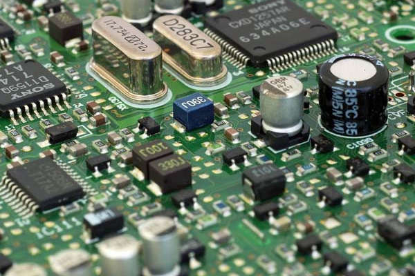
>On the path of electronic devices evolving towards high frequency and efficiency, Schottky diodes, with their revolutionary metal semiconductor junction structure, are becoming a key pivot for power management and signal processing.
Table of Contents
1、 The working principle of Schottky diode: Physical breakthrough of metal semiconductor junction
The essential difference between Schottky diodes and traditional PN junction diodes lies in their metal semiconductor contact structure:
-Barrier formation mechanism: When a metal (such as molybdenum or aluminum) comes into contact with an N-type semiconductor (silicon or gallium arsenide), electrons diffuse from the semiconductor to the metal, forming a Schottky barrier at the interface, replacing the hole electron recombination mechanism of the PN junction.
-Carrier dynamics: Only the majority of charge carriers (electrons) participate in conduction, with no minority carrier storage effect, fundamentally eliminating reverse recovery delay, and switching speed in the range of nanoseconds (typical value 1-10 ns).

Positive conduction characteristics:
-The conduction voltage is reduced to 0.15-0.45V (0.7V for silicon PN junction), reducing conduction loss by 60%.
-The low voltage drop characteristic originates from the precise control of the barrier height – the difference between the metal work function and the semiconductor electron affinity determines the barrier height, which is usually designed to be 0.6-0.8eV.
2、The role of Schottky diodes is mainly reflected in three aspects:
1. Efficient rectification
By utilizing the ultra-low forward voltage drop (0.15-0.45V) characteristic, the conduction loss in the power circuit is reduced by 60%, significantly improving conversion efficiency (such as fast charging circuits reaching over 92%).
2. High speed switch
Due to the absence of carrier storage effect, the reverse recovery time is only 1-10 ns (50 times faster than ordinary diodes), suitable for MHz level scenarios such as switching power supplies and high-frequency communication (5G/millimeter wave).
3. Protection and Continuation of Flow
Quickly conduct reverse electromotive force in inductive load circuits such as motor drives and relays to prevent voltage spikes from damaging MOSFETs/IGBTs and reduce EMI noise.
Its surface mount packaging (such as SMA/SMB) is suitable for high-density PCB layout, while the SiC material version (temperature resistant to 200 ℃) has become the core component of the new energy vehicle electronic control system. By balancing efficiency, speed, and reliability, Schottky diodes have become a key cornerstone for energy-saving and high-frequency modern electronic devices.
3、 Electrical Characteristics Advantage: Dual Evolution of High Frequency and Efficiency
1. The crushing advantage of dynamic performance
| Parameters | Schottky diode | Ordinary PN junction diode | Performance improvement benefits |
| Positive voltage drop (Vf) | 0.2-0.4V | 0.7-1.7V | Energy consumption reduced by 40-70% |
| Reverse recovery time (Trr) | <10ns | 50-500ns | High frequency switch loss reduced by 90% |
| Reverse leakage current (Ir) | 1-10mA (rising at high temperature) | 0.1-1 μ A | High temperature compensation design required |
The data comes from the comparison of actual measurements of mainstream devices in the industry
2. Irreplaceability of high-frequency applications
-In switching power supplies, in frequency scenarios above 100kHz, the reverse recovery charge (Qrr) of Schottky diodes is only 1/10 of that of PN junction diodes, significantly reducing EMI noise.
-In RF circuits (such as 5.8GHz WiFi modules), the junction capacitance is as low as 0.5-2pF to reduce signal attenuation.
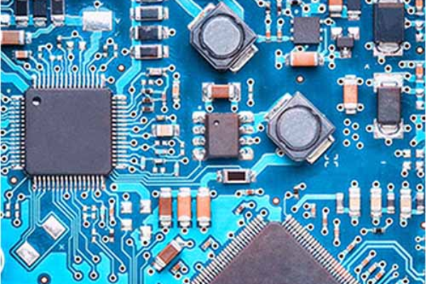
4、 Practical Guide to PCB Design: The Life and Death Line of Layout and Thermal Management
1. Layout optimization rules
-Heat source proximity:
-Power rectification scenario: Close to MOSFET (spacing<3mm), but avoid temperature sampling distortion caused by direct airflow from the heat sink.
-Automotive ECU board: In the IGBT drive circuit, a star topology is used to shorten the freewheeling path to within 5mm.
-Signal isolation design:
-Analog temperature detection circuit: The distance between the circuit and the digital power layer is greater than 2mm, and the width of the grounding wire is ≥ 0.3mm.
2. Thermal management engineering
-Copper foil heat dissipation design:
| Power level | Recommended copper foil solution | Temperature rise control target |
| <3A (SMA package) | 2oz copper foil+4 × 0.3mm heat dissipation via | Δ T<15 ℃ |
| 5-10A (TO-220) | Copper substrate+thermal conductive silicone grease gasket | Δ T < 25 ℃ |
-High temperature failure prevention:
When the ambient temperature is greater than 85 ℃, the leakage current increases exponentially (doubling every 10 ℃), and SiC Schottky tubes (with a temperature resistance of 200 ℃) need to be used.
5、 Application scenarios and selection strategies
1. Power management: the essential requirement for efficient rectification

-Mobile phone fast charging circuit: using 30V/3A patch Schottky (such as SS34), combined with synchronous rectification IC, efficiency>92%.
-Server power supply: Multiphase parallel 100V/20A dual diode (such as TO-247 package), capable of withstanding 100A transient surge.
2. Automotive Electronics: The Ultimate Test of Reliability
-LED car light drive: certified by AEC-Q101 model (such as BAS21T), resistant to vibration acceleration of 20G.
-Motor continuous current protection: The reverse withstand voltage should be ≥ twice the battery voltage (100V devices are selected for 48V systems).
3. High frequency communication: the core of the millimeter wave era
-5G millimeter wave module: Gallium Arsenide (GaAs) Schottky tube, operating frequency>30GHz, noise figure<0.5dB.
6、 Manufacturing and Process Trends: From Packaging Innovation to Material Revolution
1. Evolution of packaging technology
-Vehicle grade reliability:
-Glass passivation packaging (such as SMC): tested at 85 ℃/85% RH for 1000 hours.
-Copper lead frame: thermal resistance reduced by 40% (R θ JA ≈ 50 ℃/W → 30 ℃/W).
-Breakthrough in miniaturization:
-01005 Package (0.4 × 0.2mm): Used for TWS headphone charging case, capable of withstanding 3000 insertions and removals.
2. Iteration of material system
-SiC Schottky tube:
-The breakdown voltage is increased to 1200V (the limit of 200V for silicon tubes), and the switching loss is further reduced by 30%.
-Flexible hybrid integration:
Polyimide based Schottky array with a bending radius greater than 5mm, suitable for automotive curved radar.
Conclusion: Redefine the vitality of circuits with energy efficiency
The essence of Schottky diodes is to use quantum level contacts between metals and semiconductors to replace bulky carrier recombination – this micrometer level structural innovation has achieved the miracle of GHz level switching speed and millivolt level voltage drop. When the power efficiency of servers breaks through the titanium certification, when the range of new energy vehicles is extended by 10%, and when the fast charging of mobile phones is reduced to 20 minutes… The cornerstone of these macro improvements is the micro Schottky barrier hidden deep above the PCB.
>Intel Chief Architect Pat Kilsinger once asserted:
>Every leap in the electronics industry begins with a microscopic revolution in device physics
As a PCB manufacturer certified by IATF 16949, we provide full process support from high-frequency board selection to heat dissipation structure design. Whether you are designing a 200W server power supply or a 10 μ A IoT node, you can rely on our impedance control ± 3% and thermal management simulation capabilities to unleash the ultimate performance of Schottky diodes – because what is more important than circuit connectivity is the elegance and efficiency of energy flow.