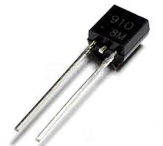
>On the core circuit board of 5G communication and radar systems, a device the size of a grain of rice is controlling the lifeline of billions of signal switches
In the rapidly developing electronics industry, PIN diodes, as a special type of semiconductor device, are increasingly becoming a key component in high-frequency circuit design. For PCB manufacturing companies, a deep understanding of the characteristics and application scenarios of PIN diodes can help engineers design higher performance circuit boards that meet the stringent requirements of modern communication, radar, and medical equipment fields.
Table of Contents
1、 Uncovering the mystery of the physical structure of PIN diodes
The essential difference between PIN diodes and traditional PN junction diodes lies in their sandwich structure:
-P-type layer: high doping concentration positive charge carrier region
-Intrinsic layer (I layer): a nearly pure layer of semiconductor material
-N-type layer: negative charge carrier region with high doping concentration
This unique structure creates its extraordinary characteristics:
-I-layer thickness: usually between 10-200 microns, directly affecting the high-frequency characteristics of the device
-Carrier lifetime: up to 1 microsecond level (ordinary diodes only have nanosecond level)
-Capacitive characteristics: can be dynamically adjusted by bias voltage
2、 Deep analysis of the three working modes of PIN Diode
1. Zero bias state (RF signal control mode)
When no DC bias is applied:
-Layer I forms a natural charge dissipation region
-Presenting high impedance characteristics (up to megaohm level)
-Equivalent to a small capacitor (0.1-2pF) connected in parallel in the circuit
2. Forward bias state (low impedance conduction mode)
When applying a forward voltage (usually>0.7V):
-Injecting a large number of charge carriers into the I layer from the P and N regions
-The conductivity of layer I has significantly increased (by up to 1000 times)
-The on resistance can be as low as 0.1-2 ohms
3. Reverse bias state (high voltage isolation mode)
When applying reverse voltage:
-Exhaustion zone extends to the entire I layer
-Generate breakdown voltage of up to kilovolts
-Extremely low reverse leakage current (nA level)
3、 Six core characteristics empower high-frequency design
1. Voltage controlled impedance characteristics:
-Impedance adjustment range: 0.1 Ω~10M Ω
-Switching time: nanosecond response speed
2. Ultra low distortion linearity:
-The third-order intermodulation intercept point (IIP3) can reach+40dBm
-Suitable for high fidelity RF systems
3. Controllable charge storage effect:
-Storage charge Q=τ × I (where τ is the carrier lifetime)
-Optimizing switch speed by designing the value of τ
4. Power processing capability:
-Continuous wave power: up to 100W (L-band)
-Peak power: tens of kilowatts (pulse application)
5. Temperature stability:
-Temperature coefficient of conduction resistance:+0.3%/℃
-Better negative temperature coefficient than ordinary diodes
6. Low harmonic distortion:
-Second harmonic suppression:<-70dBc
-Third harmonic suppression:<-80dBc
4、 Five Innovative Applications in PCB Design
1. High frequency signal switching system
In 5G Massive MIMO antenna arrays:
-Using PIN diode matrix to achieve beamforming
-Typical switching speed:<100ns
-Insertion loss:<0.5dB (6GHz frequency band)
2. Programmable attenuator network
Key points of precision attenuator design:
Circuit Example
| [RF Input] -+– [PIN1] -+– [RF Output] | | [R1] [R2] | | [PIN2]—-+ |
-Dynamic range: 0-60dB continuously adjustable
-Temperature stability: ± 0.05dB/℃
3. Limiting protection circuit
Front end protection scheme for radar receiver:
-Response time:<5ns
-Trigger power:+20dBm starting control
-Survival power: kW level pulse
4. Photoelectric detection conversion
Design of Fiber Optic Communication Receiver:
-Response bandwidth:>10GHz
-Quantum efficiency:>80% (1550nm band)
-Dark current:<1nA
5. Microwave phase control
Phased array radar phase shifter:
-Phase resolution: 5.625 °
-Insertion loss consistency: ± 0.3dB
-Power capacity: 10W average power
5、 The Golden Rule of PCB Layout
1. High frequency signal path optimization:
-Control transmission line impedance (50 Ω/75 Ω)
-Length matching tolerance:<0.1mm (millimeter wave frequency band)
2. Thermal management design:
Thermal Design Parameter Table
| Power level | Copper foil area (mm ²) | Number of vias | Heat sink requirements |
| <1W | 20-50 | 4-8 | No need |
| 1-5W | 50-200 | 12-20 | Local heat dissipation |
| >5W | >200 | 24+ | Forced air cooling |
3. Bias circuit isolation:
-Using λ/4 microstrip line to achieve DC/RF isolation
-Biased choke inductance value: ≥ 100nH
4. ESD protection strategy:
-Connect a 100 Ω resistor in series at the control end
-Parallel TVS diode (trigger voltage<5V)
6、 Trends in the evolution of cutting-edge technologies
1. Heterojunction PIN structure:
-Adopting GaAs/InP material system
-Working frequency exceeds 300GHz
-The noise figure has been reduced to 0.5dB
2. Single chip integration technology:
-Integrating multiple PIN units on a single chip
-Implement a 6-bit digital attenuator
-Reduce the size to 1 × 1mm ²
3. Silicon based PIN photodetector:
-CMOS compatible process
-3dB bandwidth increased to 50GHz
-Directly integrated with DSP chips
4. Breakthrough in High Temperature Applications:
-SiC based PIN diode
-Working temperature>300 ℃
-Suitable for aircraft engine monitoring system
In the era of millimeter wave communication and phased array radar, PIN diodes have become an indispensable core component of modern electronic systems due to their unique electrical impedance characteristics and excellent high-frequency performance. For PCB manufacturing enterprises, mastering the application technology of PIN diodes can not only improve the high-frequency performance indicators of circuit boards, but also gain opportunities in high value-added fields such as 5G base stations, satellite communications, and medical imaging.
In the next three years, the global PIN diode market is expected to expand at a compound annual growth rate of 11.2% (data source: MarketsandMarkets 2024). When your circuit board carries these tiny but powerful devices across the electromagnetic spectrum, they are redefining the boundaries of signal control – the art of electronic engineering and the pinnacle of precision manufacturing.