PCB board component assembly full process guide: 15 core processes to improve yield and reliability
Precision welding+scientific layout+intelligent detection=industrial grade PCB assembly solution
Table of Contents
1、 Key Preparation Before Assembly: Environmental and Material Control
1. Standardization of environmental parameters
-Temperature and humidity control: workshop temperature maintained at 23 ± 5 ℃, humidity<60% RH (to avoid component moisture absorption)
-Static protection: The workbench is equipped with anti-static mats (surface resistance 10 ^ 6~10 ^ 9 Ω), and the operator wears an anti-static wristband

2. Material pretreatment specifications
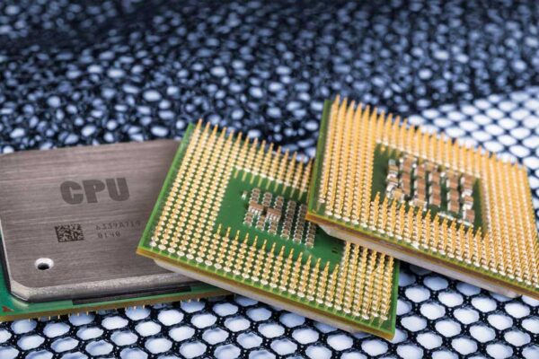
-Component baking: Humidity sensitive components (such as QFN/BGA) are baked at 125 ℃ for 12 hours (IPC/JEDEC J-STD-033 standard)
-Solder paste selection: Lead free solder paste recommended Sn96.5/Ag3.0/Cu0.5 alloy, particle size Type 3 (20-45 μ m) suitable for 0402 and above components
2、 Advanced Techniques for Welding Process of Chip Components
1. Anti monument scheme for micro components (01005/0402)
| Process parameters | Standard values | Abnormal risks |
| Pad size | L=0.25mm, S=0.15mm | Asymmetric pad causes thermal capacity imbalance |
| Steel mesh opening | 1:1 ratio | Excessive tin content causes component displacement |
| Reflow soldering slope | 2-3 ° C/s | Internal cracks caused by thermal shock |
Operation points:
-After SMT, lightly press the center of the component to increase the contact force
-Adopting a stepped heating curve: preheating at 120 ℃/90s → reflux at 220 ℃/30s → slow cooling (slope<3 ° C/s)
2. Core technology for high-density packaging and soldering
-QFN bottom pad treatment:
-The solder paste coverage of the heat sink pad should be controlled between 50% -60% (insufficient coverage can lead to poor heat dissipation, excessive coverage can cause bridging)
-Using stepped steel mesh: I/O pad thickness 0.1mm, thinning of hot pad area to 0.08mm
-0.4mm spacing QFP anti bridge connection process:
1. SPI testing after solder paste printing (thickness tolerance ± 15 μ m)
2. Use the “drag soldering method”: tilt the soldering iron tip 45 ° and drag it uniformly along the pin direction
3. Add non cleaning flux (rosin content ≥ 25%)
3、 10 golden rules for DFM manufacturability design
1. Layout avoidance guide
-Wireless module layout:
-Copper laying is prohibited below the antenna area (requires excavation)
-Stay at least 5mm away from the power module (to reduce electromagnetic interference)
-Distance between thermal sensing elements:
-The distance between the electrolytic capacitor and the heat source is ≥ 2.5mm (to prevent lifespan degradation caused by temperature rise)
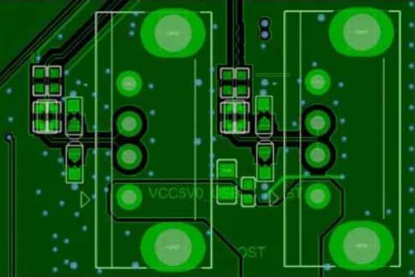
2. Solder pads and wiring specifications
| Design object | Standard parameters | Based on standards |
| 0402 component pad | Length 0.5mm/Width 0.25mm | IPC-7351B |
| Power line width (1oz copper) | 1mm/A (temperature rise of 20 ℃) | IPC-2221 |
| RF wiring | 50 Ω impedance/linewidth 0.55mm (FR4) | Applications below 3GHz |
3. Splicing and stress control
-Device direction in V-CUT region: The long side of the component is parallel to the direction of the board (reducing stress)
-Board edge safety distance: The distance between the device body and the board edge is ≥ 0.8mm, and the wiring distance is ≥ 0.5mm
4、 Welding defect diagnosis and precise repair plan
| Fault phenomenon | Root cause | Industrial grade solution |
| QFN virtual soldering | Insufficient solder paste on hot solder pads | Increase circular array holes (diameter 0.3mm) in steel mesh openings |
| BGA solder ball cracking | cooling rate too fast | adjusting reflow curve: cooling slope ≤ 2 ° C/s |
| Tin bead splashing | Insufficient solder paste temperature recovery | 4-hour constant temperature recovery (25 ℃) |
| Pin Bridge Connection | Solder Paste Collapse | Switching to High Viscosity Solder Paste (Pa · s ≥ 200) |
Repair operation specifications:
-BGA disassembly: Four corner preheating at 150 ℃ → local hot air at 380 ℃ (nozzle distance 5mm from component)
-Pad cleaning: Copper braided tape tin suction+alcohol cleaning (residue<3 μ g/cm ²)
5、 Testing certification and industry standard system
1. Level 3 testing process
-AOI detection: detection rate ≥ 99% (0201 component)
-X-Ray inspection: BGA solder joint void rate ≤ 15% (IPC-A-610 standard)
-Functional testing: High temperature aging (85 ℃/48h)+vibration testing (5-500Hz sweep frequency)
2. Core certification standards
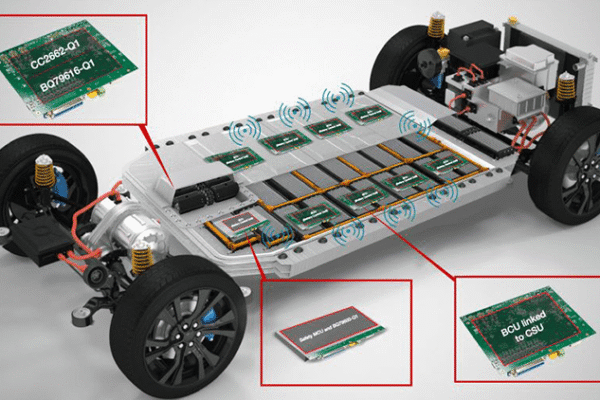
-Automotive electronics: IATF 16949 system (process defect rate ≤ 50DPPM)
-Medical equipment: ISO 13485 (MTBF ≥ 100000 hours).
Get your exclusive quote immediately: fill out the form or send an email directly.As a professional PCB manufacturer , we will provide you with a quote service within 24 hours. Enjoy free DFM optimization and a 10% discount on SMT patches for your first order!