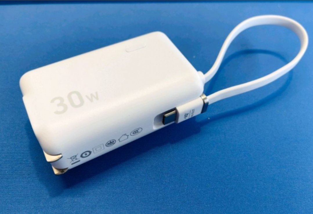
In today’s era of widespread use of portable electronic devices, the reliability, safety, and energy efficiency performance of power banks directly depend on the professionalism of their PCB design. As the “energy hub” of electronic products, the power bank PCB needs to integrate power management, multiple protections, and efficient energy conversion modules within a limited space. This article will delve into the core points of PCB design for power banks, covering key aspects such as circuit architecture, layout specifications, safety redundancy, and production compatibility, to help enterprises create more competitive power solutions in the market.
Table of Contents
1、 Design requirements and core functional modules
The power bank PCB needs to achieve complex functional integration in a compact space, and the design should prioritize meeting the following core requirements:
1. Power management system
-Charging management: supports fast charging protocols (such as PD/QC) to achieve efficient energy input;
-Discharge management: Voltage and current stability control for multi interface output (USB-A/C/Lighting);
-Battery level display: LED indicator lights or digital screen display circuit layout should avoid signal interference.
2. Battery protection mechanism
-Basic protection: overcharge, overdischarge, overcurrent, and short-circuit protection circuits (such as the DW01 chip solution);
-Enhanced protection: overvoltage, overheating, and reverse current protection to prevent damage from abnormal working conditions.
3. Interface circuit design
-Physical isolation of input/output interfaces: Type-C and other high-speed interfaces require independent copper plating to reduce crosstalk;
-Current carrying capacity: The power supply wiring width should be ≥ 1.5mm (1oz copper thickness) to avoid excessive temperature rise.
4. Space and heat dissipation optimization
-Component height restriction: It is prohibited to install ultra thick components (such as large inductors) in the battery compartment area;
-Thermal management: Distributed layout of heating elements (MOS tubes, inductors), with a heat dissipation via array added at the bottom.
2、 PCB layout specifications and taboos
A reasonable layout is a prerequisite for ensuring electrical performance and manufacturability, and the following principles should be followed:
(1) Hierarchical and Partition Strategy
-Signal isolation:
-Partition layout of high-frequency switch circuit (DC-DC conversion) and analog signal (power detection);
-Digital/analog ground segmentation, single point connection to avoid ground loop interference.
-Power layer design:
-When using a 4-layer board, the inner layer is equipped with a complete power supply/ground layer to reduce impedance;
-The power path should avoid crossing the dividing plane and reduce the current circuit area.

(2) Detailed rules for component layout
-Safety distance:
-The distance between the high voltage side (input) and the low voltage side (output) should be ≥ 3mm. If it is insufficient, slotting should be made to increase the creepage distance;
-The distance between surface mount components is ≥ 0.3mm, and the distance between the plug-in component body and the board edge is ≥ 3mm.
-Process compatibility:
-Unify the direction of wave soldering devices (horizontal/vertical) to avoid shadow effects;
-Symmetrical design of reflow soldering component pads to prevent “tombstone effect” (see legend).
>Typical error examples:
>- Right angle wiring leads to sudden impedance changes and EMI radiation;
>- Direct connection to the same network solder pad may cause the risk of soldering (should be independently led and merged).
3、 Wiring process and signal integrity
(1) Routing standards
-Line width and current carrying capacity:
| Current value | 1oz copper thickness minimum line width | Recommended line width |
| 1A | 0.3mm | 0.5mm |
| 2A | 0.7mm | 1.0mm |
| 3A | 1.2mm | 1.5mm |
-Key signal processing:
-Clock signal packet ground processing, length ≤ 25mm;
-Differential wiring (such as USB data cables) must be strictly equal in length and equidistant, with an error of ≤ 5mil.
(2) Via and pad design
-Via parameters:
-Power via hole diameter ≥ 0.3mm, welding ring single-sided ≥ 4mil;
-Avoid drilling holes on both sides of BGA solder pads to prevent stress fracture.
-Pad optimization:
-0402/0201 package uses elliptical solder pads to increase soldering reliability;
-Insert holes with “tear drops” or “hot solder pads” to improve wave soldering penetration.
4、 Safety design and reliability verification
(1) Electrical safety redundancy
-Insulation design:
-The distance between primary (AC input) and secondary (DC output) is ≥ 6.4mm, and slotting increases the distance along the surface;
-The copper spacing in the high-voltage area is ≥ 1mm, and in the low-voltage area it is ≥ 0.5mm.
-Protection circuit layout:
-The temperature sensor is placed tightly against the battery or MOS tube;
-The fuse is located near the input interface, and the wiring is shortened to reduce the circuit inductance.
(2) Key points of testing and verification
-Environmental testing:
-Verify material thermal deformation through high and low temperature cycling (-20 ℃~60 ℃);
-Insulation resistance test under 85% humidity environment.
-Electrical stress testing:
-Overvoltage/short circuit protection response time ≤ 100ms;
-Full load temperature rise test (surface temperature ≤ 70 ℃).
5、 Production adaptability design
To ensure mass production yield, it is necessary to anticipate process limitations during the design phase
1. DFM (Design for Manufacturability):
-Line width/spacing ≥ 4mil (1oz copper thickness) to avoid etching defects;
-Character height ≥ 0.8mm, width ≥ 0.1mm, ensure clear silk screen printing.
2. Layering and drilling control:
-Mechanical drilling hole diameter ≥ 0.15mm (recommended ≥ 0.3mm), tolerance ± 0.07mm;
-Laser drilling accuracy ± 0.01mm, suitable for HDI blind buried hole design.
Conclusion: Driving product value with precision design
The PCB design of power banks is a deep coupling of electronic engineering and manufacturing processes. From milliohm level on resistance optimization to ampere level current carrying, from millimeter level safety spacing to micrometer level line width control, every detail is related to user experience and product lifespan. Only by mastering the core technologies of high-density layout, multi-level protection, and intelligent power management can enterprises win the trust of users with a stable and reliable “energy heart” in fierce market competition.
>Design motto:
>An excellent power bank PCB allows complex circuits to be hidden within a compact body, ensuring safety protection runs through every millisecond of operation. ”