With the development of science and technology, most electronic products have developed to be light and compact. If electronic products want to become smaller, the electronic components used in SMT must continue to shrink in size. With the improvement of the precision of SMT placement, how to ensure the quality of solder joints has become a key concern in SMT process. The quality and reliability of solder joints can directly affect the quality of electronic products.
A good solder joint can be regarded as a solder joint whose mechanical and electrical performance can maintain stable operation during the normal service life of the equipment. The appearance of good solder joints is mostly the same:
1. The surface is complete and smooth;
2. The amount of solder is not too much or less and can completely cover the points where the pad and the lead are soldered;
3. The wetting ability is good, and the edge of the welding point is thin.
(I). Inspection of pseudo soldering method
1. Use special online testing equipment for inspection.
2. Use visual inspection or AOI inspection. If there is too little solder in the solder joints, poor solder wetting, cracks in the middle of the solder joints, convex spheres on the surface of the solder, or incompatible solder and SMD, you should immediately be vigilant to determine whether there is a pseudo solder problem in the entire batch.
Judgment method: Whether there is a problem with a large number of solder joints at the same position on the PCB board, if so, there may be a problem with the component or the pad.
(II). Causes and solutions of pseudo welding
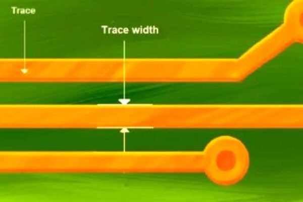
1. The pad design is defective. The pad has problems such as through holes in PAD, spacing and size is not correct, the design needs to be corrected.
2. The PCB board has been oxidized (black pads). You can use an eraser to remove the oxidized layer.
If the PCB board is damp, use a drying box to dry the PCB board.
The PCB board is contaminated by oil stains, sweat stains, etc. Use absolute ethanol to clean the PCB board.
3. After the solder paste is printed, the PCB is scratched, rubbed, etc. reduced the solder paste on the pad. Use a dispenser or use a stick to make up the solder paste in time.
4. SMD has poor quality, expired, oxidized, deformed and other conditions that cause the occurrence of pseudo welding.