Holes are a crucial part of Printed Circuit Board (PCB) manufacturing, with drilling costs accounting for 20% to 30% of the total cost. Drill bits are expensive, and after each use, some need regrinding. After several regrinds, drill bits must be discarded. Smaller drill bits require more frequent regrinding throughout their lifecycle.
In terms of function, PCB holes can be divided into two categories:
1. Via Holes (PTH Holes):
Used for electrical connections between layers.
2. Non-electrical Holes:
Used to fix or position components, which may or may not be plated based on whether electrical conduction is needed.
From a technological perspective, PCB holes are generally categorized into three types:
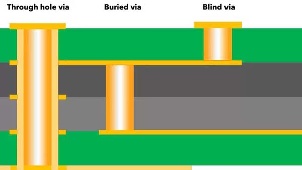
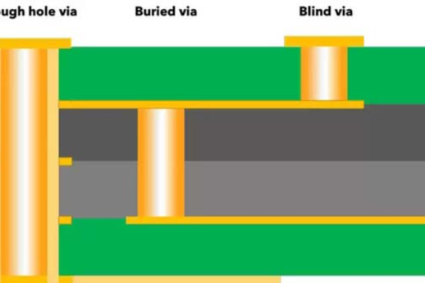
1. Blind Vias
2. Buried Vias
3. Through Holes
Table of Contents
Blind Vias
Blind vias connect the surface layer to an inner layer. At SysPCB, the depth is limited to 1-3 layers due to current laser technology capabilities. These vias do not pass through the entire board, making them ideal for high-density interconnections.
Buried Vias
Buried vias connect inner layers, such as 2 & 5 or 3 & 4 in a 6-layer PCB. These vias are entirely within the PCB and cannot be seen from the surface. To inspect buried vias, a section coupon and a microscope are used to examine the quality of the copper plating on the hole walls.
Through Holes
Through holes are mechanically drilled through the entire PCB. They can be used for internal electrical interconnections or as positioning holes for assembling components. Positioning holes are typically found on the array frame or the edge of the PCB. Most holes in a PCB are through holes due to their ease of fabrication compared to buried and blind vias.