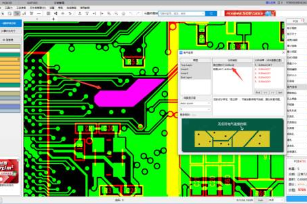
Blind via and buried via is new PCB manufacturing technology to meet the increasingly complex electronic design requirements, what are these vias and how are they different from each other, China PCB manufacturer SYS Tech will introduce as below.
The difference between blind vias and buried vias
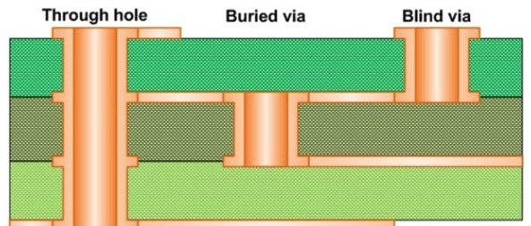
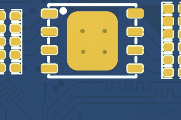
Both blind and buried vias are used for connection of different PCB layers. What are the major differences in these 2 types of vias? The blind via provides an interconnection of the outer layer with a single or multiple inner PCB layers, whereas buried via only interconnect inner layers and the buried vias are completely kept hidden and invisible from external of the PCB.
Both these vias have great advantages in HDI PCB, due to their optimal density avoid of increase in the size of board or add the number of layers in the PCB board.
4 types of PCB via holes
Blind via: the hole does not pass through the entire PCB. The blind hole always has a specified depth, which usually does not exceed a certain ratio (aperture). The literal meaning of a “blind hole” is that it is not possible to see through the hole. For example, for a 6-layer board, the drilling is only from layer 1 to layer 4. This is called a blind hole.
Buried via: buried via is a copper-plated hole that connects two or more internal layers of the board, buried via is not accessible by the external layers. it’s not possible to discover a buried via in a PCB because it is “buried” under the external layer surfaces of the board. For example, for a 6-layer board, the drilling only goes from layer 3 to layer 4, this is called buried via.
Through via: the through-holes extending from one outer layer of the PCB to another outer layer.
Component hole: holes for fixing the components on the printed board and electrically connecting the conductive patterns.