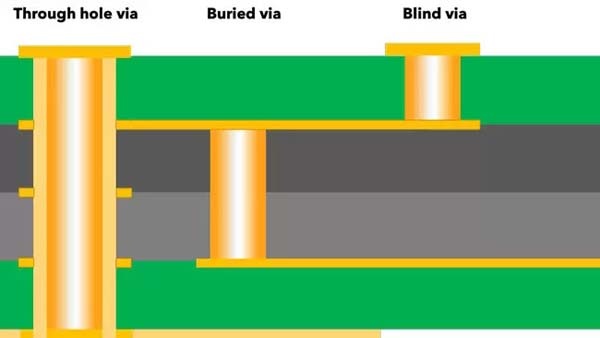
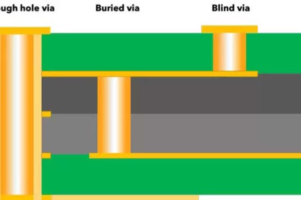
Vias are often part of the signal routing. They are vertical connections between layers to simplify trace routing around other components or when there is a high density of interconnections to be made (i.e. BGA,µBGA). As PCB trace, the PCB vias also have an associated parasitic capacitance, inductance and impedance. There is three types of Vias in PCB, Through vias, blind vias, buried vias. Among them, through vias and buried vias are mechanically drilled, blind vias are laser drilled.
Vias in high speed circuit design
1. Avoid using vias and layer changes if possible to avoid signal distortion.
2. Do not use via in high frequency clock transmission line.
3. When possible, remove any unnecessary pads on vias because these pads create parallel plate capacitance.
4. Smaller vias have lower capacitance. Short length, larger diameter vias have lower inductance. Both parasitic elements can have detrimental affects, but it is often the parasitic inductance element that provides an unexpected series impedance that creates signal transmission problems.
5. Keep the number of vias of the two differential traces the same to minimize the skew and phase difference.

Power/ground vias
For signal net, the bottleneck for the current carrying capacity is not on the via. Check the capacity on the trace (line) to get the maximum carrying capacity for the entire net.
For power net, the bottleneck is on the via, the following are some thumb of rules:
0.25mm / 0.50mm Vias with 17um / 0.5oz copper weight, the maximum safety current is 0.50A.
0.25mm / 0.50mm Vias with 35um / 1.0oz copper weight, the maximum safety current is 0.75A.
0.50mm / 1.00mm Vias with 17um / 0.5oz copper weight, the maximum safety current is 0.95A.
0.50mm / 1.00mm Vias with 25um / 1.0oz copper weight, the maximum safety current is 1.25A.
For other size or type vias, the current capacity can be estimated by equivalent trace capacity, where the trace width can be calculated by: diameter*3.14*0.6.
For example, a 0.5mm via is effectively a 0.95mm width trace on the current carrying capacity.
Thermal vias:
1. Increase plating thickness of the vias where possible to keep the thermal resistance minimum.
2. Increasing the pad size of the vias is an inexpensive way to improve the thermal spreading capacity.
3. Placing multiple small vias evenly at high power dissipation area can improve the overall thermal transfer ability comparing with one big via.
4. Vias may become filled with the solder during reflow process, this will result in less effectively of heat spreading.
5. Making solid vias, which thermally conductive material filled into them, can get lower thermal resistance. However, this adds an additional step in PCB production so extra cost will be applied.
6. Buried/blind vias have higher thermal resistance comparing with the same dimension through hole vias.
Want to make your design into real? contact SysPCB Shenzhen China, pcb manufacturer since 2006.


