In SMT (Surface Mount Technology) manufacturing, reflow soldering and wave soldering are two key soldering processes. They play different roles in the connection of electronic components and are suitable for different production needs. The following analysis will be conducted from three aspects: working principle, application field, and core differences.
Table of Contents
1、 Working principle
1. Reflow Soldering
Reflow soldering is achieved by melting pre coated solder paste, which is mainly divided into four stages:
-Preheating zone: After entering the PCB, gradually raise the temperature to 100-150 ° C, evaporate the solvent in the solder paste, and reduce thermal shock.
-Insulation zone: The temperature is stable at 150-180 ° C, and the flux is activated to remove the oxide layer, ensuring that the solder pads and component pins are wetted.

-Reflow zone: When the temperature rises to 220-250 ° C, the solder paste completely melts, and the surface tension evenly covers the solder pad and forms a reliable connection.
-Cooling zone: The solder rapidly solidifies to form stable solder joints, avoiding thermal stress damage to components.
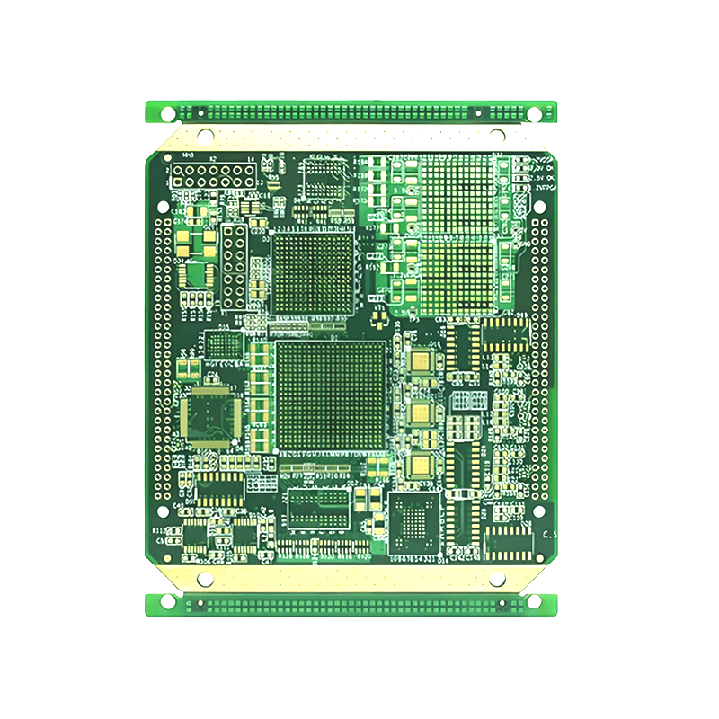
This process is suitable for surface mount components (SMD) such as chip resistors, BGA chips, etc., especially for high-density and miniaturized PCB designs.
2. Wave Soldering
Wave soldering is completed by contacting the plug pins with the wave peaks of liquid solder, and the process includes:
-Flux spraying: Spray flux on the bottom of the PCB to clean the solder pads and prevent oxidation.
-Preheating: Raise the temperature to 90-130 ° C, evaporate the solvent and activate the flux to reduce porosity during soldering.
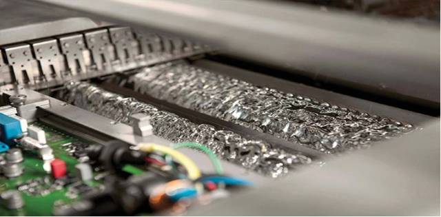
-Peak contact: The PCB passes through two solder peaks:
-Turbulent waves: High speed flowing solder penetrates dense pins, eliminating the “shadow effect”.
-Layer flow wave: Flatten solder joints, remove excess solder, and form smooth solder joints.
-Cooling: Solder solidifies, completing mechanical and electrical connections.
This process is mainly used for through-hole insertion of components (THT), such as DIP packaged chips, connectors, etc.
2、 Application Fields
-Reflow soldering:
-Applicable scenarios: motherboard soldering for miniaturized devices such as smartphones and tablets, precise connection of high-density SMD components (such as QFN, BGA).
-Advantages: High consistency of solder joints, low defect rate, and support for double-sided PCB step-by-step soldering.
-Wave soldering:
-Applicable scenarios: PCB soldering with plugins for household appliances, industrial equipment, etc., such as power modules and traditional control boards.
-Advantages: Low cost, high efficiency, suitable for rapid welding of large quantities of plug-in components.
3、 Core difference
| Comparing dimensions | Reflow Soldering | Wave soldering |
| Welding object | Surface mount components (SMD) | Flux spraying → preheating → peak contact → cooling |
| Process steps | Preheating → Reflux → Cooling | Through hole plug-in components (THT) |
| Solder form | Pre coated solder paste | Molten liquid solder |
| Equipment cost | Higher (requiring precise temperature control) | Low (suitable for large-scale production) |
| Applicable scenarios | High density, miniaturized PCB | Traditional PCB with plugins |
| Limitation | Unable to weld large-sized plugins | Not suitable for high-precision SMD components |
4、 Process selection suggestions
-Mixed assembly board: If the PCB contains both SMD and THT components, it is usually reflow soldering followed by wave soldering. Due to the possibility of plugins hindering steel mesh printing, and the high temperature of reflow soldering may damage the soldered plugins.
-Environmental trend: Both are developing towards lead-free processes, but wave soldering requires higher preheating temperatures to reduce tin slag.
Conclusion
Reflow soldering and wave soldering are two complementary technologies in electronic manufacturing. The former meets the needs of modern miniaturization with high precision, while the latter supports traditional plug-in welding with economy. Enterprises can choose reasonable process combinations based on product types, component combinations, and cost budgets to improve production efficiency and welding quality.