>Space compression of 80% and power consumption reduction of 65% – Smart watch PCB design is driving wearable electronics to the extreme of miniaturization and high performance.
Table of Contents
1、 The core challenge of PCB design for smart watches
1. Miniaturization and high-density integration
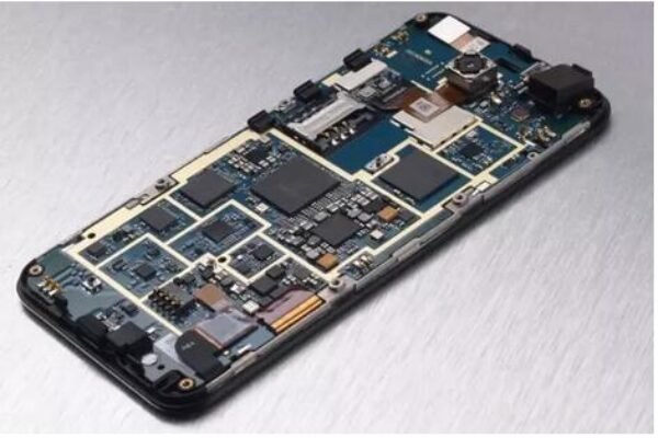
-Space limitation: The typical internal space of a smartwatch is only 5-10cm ³, and modules such as processors, sensors, and battery management need to be integrated within a 30mm x 30mm area.
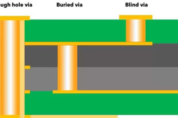
-Layer optimization: 6-8 layer HDI boards have become mainstream, with line width/spacing ≤ 3mil, and blind buried hole technology reduces the area occupied by through holes by 40%.

2. Power consumption and heat dissipation balance
-Energy efficiency bottleneck: Always on displays and biosensors account for 70% of the overall power consumption, requiring optimization of the power distribution network (PDN) impedance to<10m Ω.
-Thermal management challenge: LGA packaged chips have a thermal density of 1.2W/cm ², requiring 2oz thick copper and a heat dissipation via matrix to control temperature rise below 15 ℃.
3. Signal integrity challenge
-RF interference: Bluetooth/WiFi/GNSS antennas coexist within a 0.5mm spacing, and crosstalk suppression needs to be greater than 30dB.
-High frequency loss: The 5G millimeter wave frequency band requires PCB dielectric constant (Dk)<3.0 and loss factor (Df)<0.002.
2、 Breakthrough smartwatch PCB design strategy
1. High density interconnect (HDI) technology
-Any layer interconnection:
Replacing traditional through holes, achieving 10 μ m micro hole interconnection and increasing wiring density by 50%.
-Laser drilling optimization:
The UV laser has an accuracy of 20 μ m and supports 0.1mm BGA pitch component layout.
2. Application of Flexible Rigid Composite Plates
| Design Area | Substrate Type | Technical Advantages |
| Motherboard | Rigid FR-4 | Carrying core chips to ensure structural strength |
| Sensor module | Polyimide flexible board | Bending radius<3mm, suitable for curved surface assembly |
| Battery connector | Rigid flexible joint area | Reduce connectors, reduce thickness by 0.8mm |
>Case: A flagship watch adopts an 8-layer rigid flexible combination board, with a total thickness compressed to 1.2mm and a yield rate increased to 98.5%.
3. Advanced packaging and component integration
-SiP modularization: PMIC, MCU, and RAM are encapsulated in a 10mm × 10mm SiP, reducing wiring length by 30%.
-01005 Micro components: mounting accuracy ± 25 μ m, supporting the layout of anti noise capacitors next to heart rate sensors.
4. Low power design architecture
-Dynamic voltage regulation:
The power management IC (PMIC) provides partitioned power supply, reducing power consumption to 10 μ A in sleep mode.
-Grounding layer segmentation:
Digital/analog single point connection reduces noise by 40% (measured data).
3、 Innovation in Materials and Processes
1. Application of high-frequency materials
-LCP substrate:
Replace traditional PI flexible board, dielectric constant 2.9@10GHz Adapt to millimeter wave antenna design.
-Ceramic filled PP sheet:
The thermal conductivity has been increased to 1.5W/(m · K) to solve local overheating of the RF module.
2. Miniature component mounting

-Laser assisted positioning:
Accuracy ± 15 μ m, enabling 0201 components to be mounted on curved surfaces.
-Nano silver paste conductive adhesive:
Reduce the welding temperature to 180 ℃ to avoid thermal deformation of the flexible substrate.
3. Thermal management technology
-Embedded copper pillar:
Arranging 0.3mm diameter copper pillars at the bottom of the chip reduces thermal resistance by 60%.
-Phase change materials (PCM):
Fill the gap between the battery and the motherboard to absorb peak heat during charging and discharging.
4、 Testing and Reliability Assurance
1. Automated testing strategy
-Flying needle test+boundary scan:
The coverage rate has been increased to 99.2%, reducing testing time by 50%.
-RF OTA testing:
Verify antenna efficiency>65% and SAR value<1.6W/kg in a microwave anechoic chamber.
2. Environmental adaptability design
-Waterproof structure:
The thickness of the solder mask layer is ≥ 25 μ m and has passed IP68 certification (1.5m water depth/30 minutes).
-Bending fatigue test:
The resistance change of the flexible PCB after 100000 bending cycles is less than 5%.
5、 Future Trends: AI Driven and Heterogeneous Integration
1. AI optimized design process
-Machine learning algorithms predict wiring conflicts, reducing the HDI design cycle from 14 days to 5 days.
-The digital twin model simulates a drop impact, with a PCB life prediction error of less than 5%.
2. Breakthrough in Heterogeneous Integration
-3D stacked silicon interlayer:
The memory is vertically interconnected with the processor, and the data transfer rate is increased to 8Gbps.
-Embedded passive components:
Resistors/capacitors are embedded in the substrate, releasing 15% of the surface wiring space.
Conclusion: Empowering Next Generation Wearable Device Innovation
>By 2025, the global shipment of smart watches will exceed 210 million pieces (Statista data), with high density, low power consumption, and strong anti-interference becoming the core indicators of PCB design.
SysPCB provides:
-Free design review: Submit schematic and obtain DFM/DFA report (including impedance control and thermal simulation data) within 48 hours
-Quick sampling service: 24-hour delivery of 6-20 layers of HDI boards, supporting 0.1mm laser drilling and rigid flexible bonding process
-Full process support: one-stop delivery from layout design to SMT placement, with a yield commitment of 99.2%
Take immediate action: Upload your smartwatch PCB design requirements and receive the “Wearable Device PCB Design White Paper”+enjoy free HDI engineering fees for your first order!