The incoming inspection of PCB materials in SMT factories is a key step in ensuring the quality of subsequent SMT patches and reducing production abnormalities (PCB quality defects may lead to issues such as virtual soldering, short circuits, component offset, etc.). The inspection process should combine the four core dimensions of appearance, size, electrical performance, and process adaptability, while following standardized sampling and judgment rules. The following is the detailed process and inspection content:
Table of Contents
1、 SMT incoming PCB inspection process
The overall process follows a closed-loop logic of “receiving → information verification → sampling → full item inspection → judgment → processing”, with the following specific steps:
1. Reception and information verification
-When receiving PCBs in the warehouse, the first step is to check the “Purchase Order”, “PCB Specification”, and physical identification (model, batch number, quantity), confirm that they are correct, and then register them in the waiting area (hang the “waiting for inspection” label).

-Check packaging integrity: PCBs are usually packaged in anti-static bags+trays/partitions, and it is necessary to confirm that there is no compression deformation or moisture (the packaging bag is not damaged, and the desiccant is effective). FPC needs to be additionally checked for anti folding protection measures (such as hard liners).
2. Development of Sampling Plan
-According to GB/T 2828.1 (Sampling Inspection Standards by Attributes), determine the AQL level based on the importance of PCB (such as core board, ordinary board):
-Fatal defects (such as short circuits and open circuits): AQL 0 (zero defect acceptance);
-Main defects (such as pad oxidation, positioning hole offset): AQL 1.0;
-Minor defects (such as minor scratches, blurry characters): AQL 2.5.
-When the batch size is ≤ 500 pieces, the sampling quantity is ≥ 30 pieces; When the batch size is greater than 500 pieces, the sampling size is calculated as “batch square root x 2” (e.g. 63 pieces are taken out of 1000 pieces).
3. Conduct a comprehensive inspection
-Inspect in the order of “appearance → size → electrical performance → process adaptability”, use specialized tools (such as AOI, caliper, impedance meter) and record the data.
4. Comprehensive judgment

-If the number of defects in the sampling does not exceed the AQL acceptance value, it is judged as “qualified” and transferred to the qualified area (marked as “qualified”);
-If the allowable value is exceeded, it will be judged as “unqualified”, isolated, and the review process will be initiated (see step 5).
5. Handling of non-conforming products
-Identification isolation: hang the “unqualified” label, record the defect type, quantity, and batch to avoid misuse;
-Review decision: jointly reviewed by the quality, engineering, and procurement departments to determine the handling method (rework repair, special procurement use, batch rejection);
-Feedback improvement: Provide defect data to PCB suppliers, request submission of corrective and preventive actions (CAPA), and track and verify.
2、 Core inspection content (classified by inspection dimensions)
1. Appearance quality inspection (the most basic and high-frequency source of defects)
-Substrate surface:
-No obvious scratches (depth>0.05mm is considered a defect), indentations, dents, oil stains, fingerprints, metal shavings or other contaminants (visible after wiping with a dust-free cloth is still considered unqualified);
-No delamination or bubbles (between the substrate and the copper foil/solder mask), especially around the corners and via holes (defects with bubble diameter>0.5mm).
-Solder pads and wires:
-The solder pads (including BGA solder pads and QFP solder pads) are free of oxidation (appearing dull/black, which can be tested by tin wiping: using a soldering iron dipped in tin to gently wipe, can evenly apply tin to be qualified), free of damage (gaps greater than 10% of the solder pad area are defects), and free of burrs (affecting the surface mounting accuracy);

-The wire has no broken wires or exposed copper (not covered by the solder mask), and the line width deviation is ≤ ± 10% of the design value (if designed to be 0.2mm, the actual measurement should be within 0.18-0.22mm).
-Solder Mask:
-Uniform color (no localized yellowing/whitening), good adhesion (peeled off with 3M tape without detachment);
-Accurate window opening: The solder mask in the pad area is not covered (with a coverage area greater than 5%, the pad is a defect), and there is no missing window opening in the non pad area (to avoid accidental soldering);
-No bubbles or pinholes (diameter>0.2mm is considered a defect to prevent solder overflow and short circuit).
-Character (Silk Screen):
-Clear and distinguishable (without blurring or missing pen), with a positional deviation of ≤ 0.2mm (to avoid misleading manual inspection);
-Adhesion meets the standard (no detachment after peeling off 3M tape).
-Holes (positioning holes, conductive holes):
-No blockage (the conductive hole needs to be 100% conductive and can be checked with a probe), no deformation (aperture deviation ≤± 0.05mm);
-The positional deviation of the positioning hole is ≤ 0.05mm (which affects the SMT equipment placement, and excessive deviation can cause component displacement).
2. Dimensional and positional tolerance inspection (to ensure assembly and surface mounting accuracy)
-External dimensions:
-Measure the length and width with a digital vernier caliper (accuracy 0.01mm), with a deviation of ≤ ± 0.1mm of the design value (if the design is 50mm, the actual measurement is 49.9-50.1mm);
-The thickness is measured with a micrometer (accuracy 0.001mm), with a deviation of ≤± 0.05mm (affecting the assembly with the shell and the fit with the steel mesh).
-Positioning hole:
-Aperture: measured with a plug gauge, with a deviation of ≤± 0.05mm (if designed with a diameter of 2.0mm, a diameter of 1.95mm plug gauge is required, not a diameter of 2.05mm);
-Hole location coordinates: use the anime image measuring instrument to detect, and the deviation from the designed CAD coordinates is ≤ 0.05mm (to prevent MARK point identification deviation when mounting).
-Warping degree (key indicator, directly affecting the quality of the patch):
-Testing method: Place the PCB flat on a marble platform and measure the maximum gap with a feeler gauge;
-Standard: Rigid PCB warpage ≤ 0.75% (e.g. 100mm long PCB, maximum gap ≤ 0.75mm); FPC bending radius ≥ design value (usually ≥ 3mm to avoid breakage at bends).
-Verticality of board edge:
-Check with a square ruler to ensure that the verticality deviation is ≤ 0.1mm/m (to prevent the edges from tilting after the separation of the panels, which may affect assembly).
3. Electrical performance testing (to avoid implicit functional defects)
-Conductivity and short circuit (100% sampling or critical network testing):
-Use a flying needle testing machine or ICT testing fixture to check whether all networks are conductive (without open circuits) and whether adjacent networks are insulated (without short circuits);
-Insulation resistance standard: ≥ 100M Ω at room temperature (500V DC test), ≥ 10M Ω in humid environment (40 ℃/90% RH).
-Impedance control (for high-speed signal PCBs, such as boards with Bluetooth and DDR):
-Use an impedance tester (such as TDR time domain reflectometer) to test the characteristic impedance of key differential lines (such as USB, LVDS) and single ended lines, with a deviation of ≤ ± 10% of the design value (if the design is 100 Ω, it should be within 90-110 Ω);
-Test points need to be reserved at the edge of the PCB (according to design specifications) to ensure testing accuracy.
-Via quality (for multi-layer boards, HDI boards):
-Blind buried hole conductivity: Use an X-ray detector to check whether the coating inside the hole is continuous and free of voids (void area>10% of the hole wall is a defect);
-Plug hole quality: The resin plug hole should be flat (protruding surface ≤ 0.05mm), without dents, to prevent solder from penetrating into the hole and causing virtual soldering.
4. Process adaptability testing (matching SMT production process)
-Surface treatment process (directly affecting solder wettability):
-Confirmation of surface treatment type: check whether it is consistent with the order (such as immersion gold, OSP, tin spraying, nickel plating);
-Coating thickness: The thickness of the deposited gold layer is ≥ 0.05 μ m (ENIG process), the thickness of the OSP film is 0.2-0.5 μ m (too thin is prone to oxidation, too thick affects tin deposition), and the thickness of the sprayed tin layer is 5-15 μ m (no missed spraying, low tin);
-Solderability test (sampling for soldering test): Dip the solder pad in flux and immerse it in a 235 ± 5 ℃ soldering furnace. After 5 ± 0.5 seconds, remove it and ensure that the soldering area is ≥ 95% (IPC-A-610 standard).
-MARK point (SMT patch positioning reference):
-Appearance: MARK dots (circular, usually with a diameter of 1.0-1.2mm) are free of oxidation and oil stains, and have a smooth surface (with consistent reflection for easy equipment identification);
-Size and position: Diameter deviation ≤ ± 0.05mm, center coordinate deviation from design ≤ 0.05mm, no solder mask or characters within 2mm around (to avoid recognition interference).
5. Material and identification inspection (compliance and traceability)
-Material confirmation:
-Check whether the PCB substrate model (such as FR-4, Rogers 4350) and number of layers (such as 4-layer board) are consistent with the order (can be judged by the supplier’s material certificate and appearance, such as FR-4 being light yellow and high-frequency boards mostly being white);
-Flame retardant rating: Must comply with UL94 V-0 (burned with a lighter for 10 seconds, extinguished within 30 seconds after leaving, no dripping).
-Clarity of identification:
-The PCB should have the model number, batch number, supplier logo (traceable to the source), character height ≥ 0.8mm, width ≥ 0.2mm, and no overlap or blurring.
3、 List of Inspection Tools
| Inspection items | Tool types | Accuracy requirements |
| Appearance defects | Magnifier (10x), AOI equipment | Identify defects above 0.1mm |
| Size/hole location | digital caliper, anime camera | 0.01mm/0.001mm |
| Curvature | Marble platform, feeler gauge | 0.01mm |
| Conduction/short circuit | Flying needle testing machine, ICT fixture | Detecting open circuits below 1 Ω |
| Impedance | TDR Impedance Tester | ± 1 Ω |
| Coating thickness | Film thickness gauge (X-ray fluorescence method) | ± 0.01 μ m |
4、 Key precautions
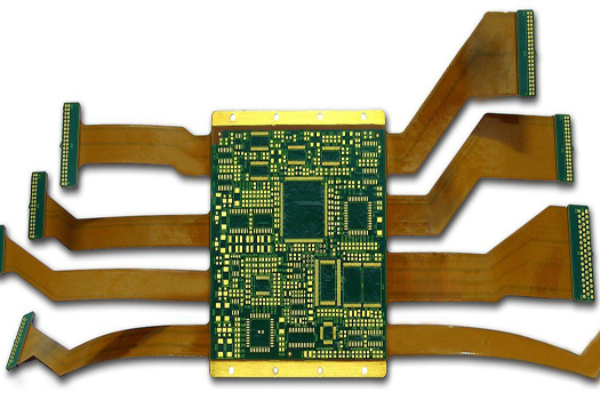
-FPC special inspection: Additional inspection is required to check whether there are micro cracks in the bent area of the circuit (using a microscope), whether the reinforcement plate is firmly attached (tensile force ≥ 5N), and whether the gold finger coating is uniform (without exposed copper).
-Batch consistency: The color and surface treatment glossiness of PCBs in the same batch should be consistent (to avoid mixing or quality differences between different batches).
-Environmental control: The inspection area needs to be anti-static (grounding resistance 1-100 Ω) and dust-free (Class 10000) to avoid secondary pollution or damage to the PCB during the inspection process.
Through the above process and content inspection, PCB incoming defects can be effectively intercepted, laying the foundation for high yield of SMT surface mount.
Get your exclusive quote immediately: fill out the form or send an email directly.As a professional PCB manufacturer for hobbyist , we will provide you with a quote service within 24 hours. Enjoy free DFM optimization and a 10% discount on SMT patches for your first order!


