The production process of SMT processing has certain requirements for the layout of components. Different processes, such as wave soldering, single-sided reflow soldering, double-sided reflow soldering, etc., have different requirements. Below, Shenzhen SYS Technology, a SMT processing manufacturer, briefly introduces the requirements for layout of components during SMT assembly.
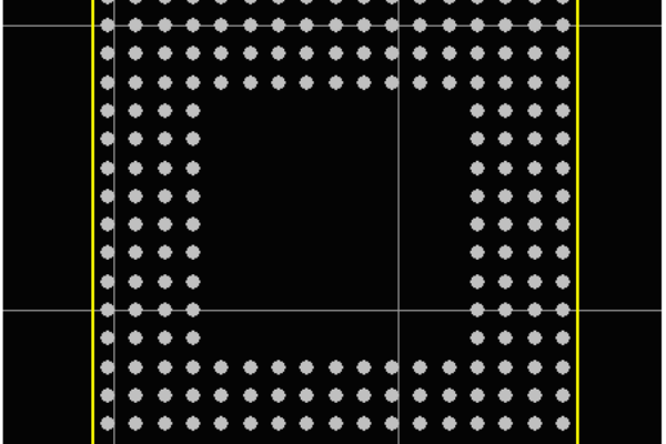
1. The distribution of components on the PCBA should be as even as possible.
2. Arrangement angle of electronic components on the PCB, the same type of electronic components should be arranged at the same angle as much as possible, and the characteristic angle should be kept consistent, which is conducive to the mounting, soldering and testing of electronic components.
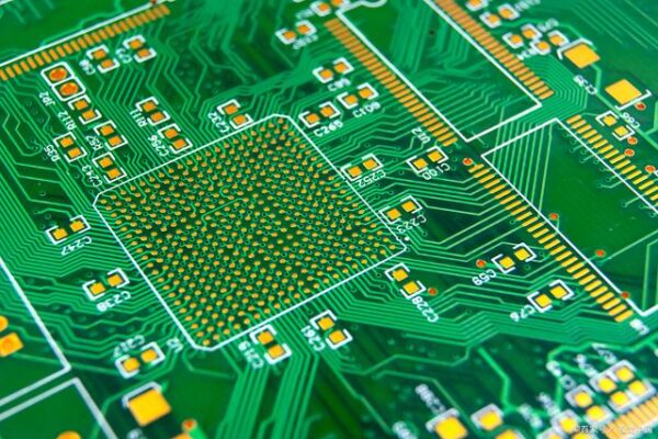
3. It should be vacant around the large electronic components, such as BGA, QFP etc., so that the SMD rework equipment with big heating header that can be operated on it.
4. Heat radiating electronic components should be as far away as possible from other electronic components, usually placed in the corners, ventilated positions in the chassis. Heat radiating electronic components should be supported by other leads or other supports (for example, heat sinks can be added) to keep the heat-generating electronic components and the PCB surface at a certain distance, with a minimum distance of 2 mm.
5. Temperature sensitive electronic components should be kept away from heating radiating electronic components.
6. The layout of electronic components and parts that need to be adjusted or replaced frequently, should be considered with the whole structure of the equipment requires, such as potentiometers, adjustable inductance coils, variable capacitor micro switches, fuses, buttons, plugs and other electronic components, should be placed in a position conducive to adjustment and replacement.
7. Fixing holes should be arranged near the connection terminals, plug-in parts, and the center of the long series of terminals where the force is often applied from time to time. At the same time, a corresponding space should be reserved around the fixing holes to avoid deformation due to thermal expansion.
8. The distance between some electronic components, spare parts and other electronic components that require secondary processing due to large volume tolerances and low precision is increased by a certain margin on the basis of the original setting.
9. It is recommended that the margin of electrolytic capacitors, varistors, bridge stacks, polyester capacitors, etc. is not less than 1mm, and transformers, radiators and resistances exceeding 5W (including 5W) are not less than 3mm.
10. Electrolytic capacitors should not touch heating electronic components, such as high-power resistance thermistors, transformers, radiators, etc.
11. The stress-sensitive electronic components cannot be placed on the corners, edges of the PCB or near the connectors, mounting holes, slots, cutouts, gaps and corners.
12. The layout of electronic components must meet the process requirements and spacing requirements of reflow soldering and wave soldering.
13. The PCB positioning hole and the position occupied by the fixing bracket should be vacated.
14. In the large-area PCB design plan with an area exceeding 500cm2, in order to avoid PCB bending when passing through the reflow furnace, a 5~10mm wide gap should be left in the middle of the PCB without electronic components (wires can be routed). In order add press bar to avoid PCB bending when going through the tin furnace.
I. The placement angle of electronic components should take into account the angle at which the PCB enters the reflow oven.
II. The long axis of the two end chip electronic components on the PCBA should be perpendicular to the angle of the conveyor belt of the reflow oven.
III. The long axis of the SMD electronic components should be parallel to the transmission angle of the reflow oven, and the long axis of the Chip electronic components at the two ends and the long axis of the SMD electronic components should be perpendicular to each other.
IV. A good layout design plan of electronic components should take into account the symmetrical heat capacity and the arrangement angle and order of the electronic components.
V. For large-size PCBs, in order to keep the temperature on both sides of the PCB as consistent as possible, the long side of the PCB should be parallel to the angle of the conveyor belt of the reflow oven.
15. Installation spacing of electronic components: The minimum installation spacing of electronic components must meet the manufacturability, testability and maintainability requirements of SMT assembly.