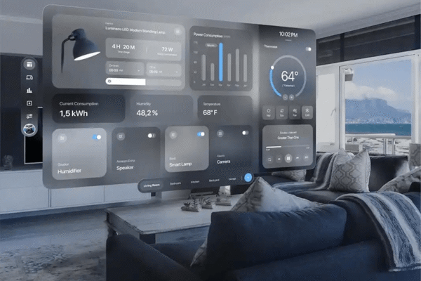
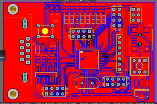
PCB size is determined according to the size of the overall structure of the machine case. PCB size and shape should be suitable for PCB manufacturing lines, applicable size of surface assembly machine and reflow oven operating width.
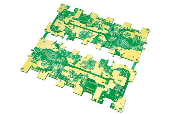
If PCB size is small, in order to better adapt to the SMT automated production, often combine multiple boards into one board, several same PCB are put together regularly, in rectangular or square shape, the multiple PCBs in rectangular or square shape are know as PCB panel.
Arrange small size PCB in to panel can improve production efficiency, enlarge applicability of the production line, reducing tooling preparation costs.
Single side surface-mount PCB need arrange the components side in same side, double side surface-mount pcb (no need of wave-soldering) can be positive and negative arrangement for each half, both sides in the same quantity arrangement.
positive and negative arrangement can improve equipment utilization (in medium and small batch production can save half cost), also reduce production preparing time.
One can use straight V-shaped groove, stamp holes, punching and other technology means or their combinations to connect each small PCB, connecting requiring precise registration, uniform V-grooving depth, with good mechanical strength but easy to break apart by machine or by hand.
For different small PCB these methods can be also used, but should pay attraction to the way of element marking.
Panel of the printed circuit board, commonly known as “stamp” board:
1. Stamp board may be the same PCBs or different PCBs composition.
2. Many factors determine the maximum dimensions of the stamp PCB, such as the Max. effective area of pick&place machine, paste printer’s Max. printing area and Max. width of reflow conveyor.
3. Stamp connectors provide mechanical support between boards and edges of “stamp” board .Therefore connectors should have certain strength, but also easy to be break apart from each circuit.