In modern electronic systems, the microcontroller control board serves as the core component, undertaking key tasks such as data processing and signal control. The quality of its design directly affects the performance, reliability, and stability of the entire system. In order to create a high-quality microcontroller control board, a series of important principles need to be followed in the design process.
Table of Contents
1、 Hardware design principles
(1) Reasonable chip selection
Chip selection is the primary step in the design of microcontroller control boards. Choose the appropriate microcontroller model based on specific application requirements. Consider the performance parameters of the microcontroller, such as computing speed, storage capacity, peripheral interfaces, etc. For applications that require high computing speed, such as real-time data processing, high-speed communication, etc., a microcontroller with high-performance CPU core and high clock frequency should be selected.

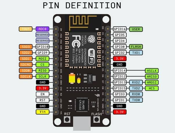
In the image recognition processing of intelligent cameras, it is necessary to quickly process a large amount of image data. In this case, selecting a microcontroller with fast computing speed can ensure the real-time performance of image recognition. In terms of storage capacity, if the application program is complex and the data volume is large, it is necessary to choose a microcontroller with large Flash and RAM to meet the requirements of program storage and data processing. Also pay attention to the peripheral interfaces of the microcontroller, such as whether it has commonly used interfaces such as UART, SPI, I2C, etc., to facilitate communication and connection with other external devices.
(2) Optimize circuit layout
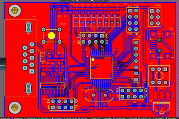
Reasonable circuit layout is crucial for improving the performance of microcontroller control boards. When laying out, the microcontroller should be placed as close as possible to key circuit components such as crystal oscillators and reset circuits to reduce signal transmission paths and signal interference. As a key component that provides clock signals for microcontrollers, the connection line between the crystal oscillator and the microcontroller should be as short and thick as possible to reduce line impedance and ensure the stability of the clock signal. For power circuits, reasonable zoning design should be carried out to separate the layout of power circuits with different voltage levels and avoid mutual interference. In the design of multi-layer circuit boards, it is necessary to plan the power layer and ground layer reasonably, and reduce the internal resistance and ground potential difference of the power supply through large-area copper laying, in order to improve the anti-interference ability of the system. At the same time, attention should be paid to the direction of signal lines to avoid signal crossings, sharp angles, and reduce signal reflections and crosstalk.
(3) Power stability design
A stable power supply is the foundation for the normal operation of the microcontroller control board. When designing power circuits, it is important to ensure the stability of the power output voltage and sufficient current carrying capacity. Select appropriate power chips and filtering capacitors based on the power consumption requirements of microcontrollers and other peripherals. For some circuits that are sensitive to power noise, such as analog circuits, specialized power filtering and voltage regulation measures should be adopted. LC filtering circuits, linear voltage regulation chips, etc. can be used to minimize power noise. At the power input port, overvoltage and overcurrent protection circuits should be installed to prevent damage to the control board due to external power supply abnormalities. When the power supply voltage is too high, the overvoltage protection circuit can automatically cut off the power input; When the current is too high, the overcurrent protection circuit can limit the current and protect the components on the control board.
2、 Principles of Software Design
(1) Modular programming
Adopting modular programming ideas can make the program structure clear, easy to maintain, and expand. Divide the entire application into multiple independent modules based on their functions, such as data acquisition module, communication module, control algorithm module, etc. Each module is responsible for specific functions and has independent code and interfaces. The data acquisition module is responsible for obtaining data from sensors and performing preliminary processing and conversion; The communication module is responsible for data transmission with external devices and can use communication protocols such as UART and SPI. Modular programming reduces the coupling between different modules, so that when a module needs to be modified or upgraded, it will not affect the normal operation of other modules. In the later maintenance and functional expansion of the product, it is easy to optimize and improve individual modules, thereby improving development efficiency.
(2) Efficient algorithm design

In the software design of microcontroller control boards, the efficiency of algorithms directly affects the performance of the system. Design efficient algorithms based on specific application requirements. In terms of control algorithms, it is necessary to choose appropriate control strategies, such as PID control algorithm, which is widely used in the field of industrial control. By adjusting PID parameters reasonably, precise control of the controlled object can be achieved.
In data processing algorithms, attention should be paid to the time and space complexity of the algorithm. For applications that require processing large amounts of data, such as data collection and analysis systems, using efficient data processing algorithms can reduce data processing time and improve system real-time performance. At the same time, it is necessary to avoid algorithms that are too complex, so as not to occupy too many microcontroller resources and affect the overall performance of the system.
(3) Reliability and fault-tolerant design
The reliability and fault tolerance of software are key to ensuring the stable operation of the microcontroller control board. In programming, necessary error detection and handling mechanisms should be incorporated. In the process of data collection, it is necessary to verify the validity of the collected data. When abnormal data is detected, error prompts and processing should be carried out in a timely manner. This can be achieved by setting flags, sending error messages, and other methods to notify the system for corresponding processing. For some possible abnormal situations, such as power failure, communication interruption, etc., corresponding fault-tolerant handling programs should be designed. When the power fails, timely save important data so that the system can quickly resume operation after the power is restored; Automatically attempt to re-establish communication connection during communication interruption to ensure uninterrupted operation of the system.
3、 Reliability design principles
(1) Anti interference design
The microcontroller control board often faces various interferences in practical applications, such as electromagnetic interference, power supply noise interference, etc. Therefore, anti-interference design is crucial. In terms of hardware, in addition to optimizing circuit layout and power stability design as mentioned earlier, measures such as shielding and filtering can also be adopted. For some sensitive circuit parts, such as analog signal input and output ports, metal shielding covers are used for shielding to reduce the impact of external electromagnetic interference. In terms of software, software filtering algorithms can be used to filter the collected data and remove noise interference. For some important control signals, multiple verifications, redundant transmission, and other methods can be used to ensure the accuracy and reliability of the signals.

(2) Hot Design
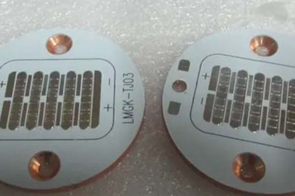
During the operation of the microcontroller control board, the chip and other components generate heat. If the heat cannot be dissipated in a timely manner, it will cause the chip temperature to be too high, affecting its performance and lifespan. Therefore, it is necessary to carry out reasonable thermal design. When arranging components, place components with high heat generation, such as power chips, in positions that are conducive to heat dissipation, such as near ventilation openings or heat sinks. For some chips with high power consumption, heat sinks or fans can be installed for forced heat dissipation. At the same time, the heat dissipation capacity of the circuit board should be considered, and the material and thickness of the circuit board should be selected reasonably to improve its heat dissipation performance.
4、 Cost control principle
(1) Component selection and cost balance
Reasonably control component costs while meeting design requirements. When selecting chips, do not blindly pursue high-performance and high price chips, but choose chips with high cost-effectiveness according to actual application needs. For some application scenarios that do not require particularly high performance, a low-cost general-purpose microcontroller can be chosen. When selecting other peripheral components, cost accounting should also be conducted to avoid using overly expensive components. However, it should be noted that cost reduction cannot be achieved at the expense of product quality and reliability. A balance must be found between component selection and cost.
(2) Production process and cost optimization
The choice of production process will also affect the cost of the microcontroller control board. In the design phase, the feasibility and cost of production processes should be considered. Adopting standard surface mount technology can improve production efficiency and reduce production costs. Efforts should be made to minimize the use of special processes and components, such as plug-in components that require manual welding. This not only increases production time and labor costs, but may also affect product consistency and reliability. By optimizing the design of the circuit board to meet the requirements of large-scale production, production costs can be effectively reduced.
The design of a microcontroller control board is a comprehensive project that requires adherence to various principles such as hardware design, software design, reliability design, and cost control. Only by fully considering these principles in the design process can a high-performance, stable, reliable, and cost-effective microcontroller control board be designed to meet the needs of different application scenarios and promote the development and application of electronic systems. In future design practices, with the continuous development of electronic technology, it is necessary to constantly explore and update design principles to adapt to new technological challenges and market demands.
Get your exclusive quote immediately: fill out the form or send an email directly.As a professional PCB manufacturer for hobbyist , we will provide you with a quote service within 24 hours. Enjoy free DFM optimization and a 10% discount on SMT patches for your first order!


