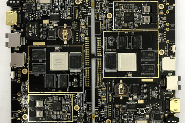
A standard 2-layer PCB (Printed Circuit Board) is one of the most commonly used types in electronic products, offering a balance between complexity, cost, and functionality. Unlike single-layer PCBs, 2-layer boards feature conductive traces on both sides, allowing for more complex circuit designs. This article outlines the complete production process of a standard 2-layer PCB, from design to final inspection.
Table of Contents
1. PCB Design and Preparation
The process begins with designing the PCB layout using CAD (Computer-Aided Design) software such as Altium Designer, Eagle, or KiCad. Key design considerations include:
Layer stack-up definition (Top layer, Bottom layer, dielectric layer)
Trace width and spacing based on electrical requirements
Pad and via placements
Gerber file generation for manufacturing
2. Raw Material Selection
A standard 2-layer PCB typically uses FR-4 (fiberglass-reinforced epoxy laminate) as the base material, offering excellent electrical insulation and mechanical stability. The board consists of:
Copper foil layers (35μm or 1oz standard thickness)
Prepreg and core layers for dielectric insulation
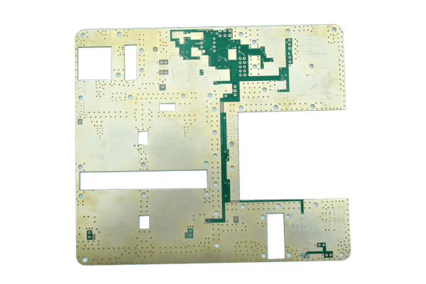
3. Copper Clad Laminate Preparation
The manufacturing process starts with copper-clad laminates, where a thin copper layer is bonded to both sides of an insulating core. These sheets serve as the foundation for the circuit pattern.
4. Circuit Pattern Transfer
Photoresist Application and Exposure
A light-sensitive photoresist is applied to the copper surface.
The board is exposed to UV light through a photomask that contains the circuit design.
The exposed areas harden, while the unexposed areas remain soluble.
Etching Process
The board is immersed in an etching solution (typically ferric chloride or ammonium persulfate) to remove unprotected copper.
The hardened photoresist is then stripped away, leaving behind the desired copper traces.
5. Drilling and Plating
Drilling Holes
Precision CNC machines drill vias, component holes, and mounting holes.
Hole diameters are determined by component lead size and via requirements.
Through-Hole Plating
To create electrical connections between layers, holes are plated with a thin layer of copper (electroless plating).
Additional electroplating increases the copper thickness for reliability.
6. Solder Mask Application
A solder mask is applied over the copper traces to protect against oxidation, short circuits, and accidental solder bridging. The process includes:
Coating the board with a green (or other color) solder mask layer.
UV exposure and development to remove unwanted solder mask from pads and vias.
Curing to harden the protective layer.
7. Silkscreen Printing
A silkscreen layer is printed onto the board for component labeling, reference designators, and logos. This helps with assembly and troubleshooting.
8. Surface Finish Application
To improve solderability and protect exposed copper, a surface finish is applied. Common types include:
HASL (Hot Air Solder Leveling) – Low-cost and widely used.
ENIG (Electroless Nickel Immersion Gold) – Provides better oxidation resistance.
OSP (Organic Solderability Preservative) – Environmentally friendly but less durable.
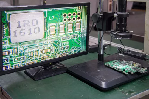
9. Final Inspection and Testing
Before shipment, the PCB undergoes strict quality control checks:
Automated Optical Inspection (AOI) for detecting defects.
Electrical Testing (Flying Probe or Bed-of-Nails Test) to verify circuit connectivity.
Final visual inspection for surface defects, solder mask alignment, and overall board quality.
10. PCB Cutting and Packaging
The finished PCBs are cut from the manufacturing panel using V-scoring or routing.
Cleaned and packaged properly to prevent contamination and mechanical damage.
Conclusion
The standard 2-layer PCB production process involves multiple precise steps, from design to final inspection. Each stage, including material selection, pattern etching, drilling, plating, and finishing, contributes to the overall quality and functionality of the board. Understanding this process helps designers and engineers optimize their PCB layouts for manufacturability and reliability.