> A single millimeter of PCB warpage can increase SMT defect rates by 40%—making warpage control a critical cost and reliability factor in high-density electronics manufacturing.
In the high-stakes world of PCB fabrication, warpage (the deviation from perfect flatness) isn’t merely a cosmetic flaw—it’s a multi-million-dollar reliability threat. As components shrink and thermal demands escalate, warpage-induced failures account for over 25% of SMT assembly defects globally. This article reveals actionable strategies to master warpage control while meeting IPC’s stringent <0.75% flatness standards.
Table of Contents
1. Warpage Origins: Thermal, Material, and Design Triggers
1.1 Thermal Stress: The Primary Culprit
– CTE Mismatch: Copper (17 ppm/°C) and FR-4 (12–16 ppm/°C) expand at different rates. At reflow temperatures (220–250°C), this mismatch generates shear stresses up to 150 MPa—enough to deform thin PCBs permanently .
– Rapid Thermal Cycling: Thermal shock during soldering—especially lead-free processes with 250°C peaks—exceeds Tg points, allowing permanent deformation .

1.2 Material and Process Defects
– Moisture Absorption: Non-RoHS-compliant laminates absorb humidity, swelling by 0.3% at 60% RH and warping during reflow .
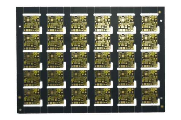
– Uneven Copper Distribution: Asymmetric copper coverage (e.g., 80% on top vs. 20% bottom layer) creates imbalanced stresses, warping boards like a bimetallic strip .
– V-Cut Stress Concentration: V-scoring depths >1/3 board thickness fracture fiberglass weaves, reducing panel rigidity by 30% .
1.3 Design and Manufacturing Oversights
– Insufficient Board Thickness: 0.6mm ultra-thin PCBs warp 3× more than 1.6mm boards under identical thermal loads .
– Improper Storage: Stacking PCBs vertically without support induces creep deformation over time .
2. The High Cost of Warpage: From Assembly Failures to Field Returns
2.1 SMT Assembly Disasters

– Misaligned Components: Warpage >0.5mm causes 0201 capacitors/chips to shift during placement, creating bridges or opens .
– Head-in-Pillow Soldering: Warped BGA substrates prevent ball-to-paste contact, increasing voiding rates by 50% .
2.2 Performance and Reliability Impacts
– Signal Integrity Loss: 0.3mm warpage alters impedance by ±8Ω in 100GHz RF boards, causing timing jitter .
– Thermal Runaway: Warped boards reduce heatsink contact by 60%, elevating MOSFET temperatures by 15°C+ .
– Mechanical Fatigue: Cyclic warpage stresses fracture solder joints, accelerating failure in automotive/vibration environments .
3. Warpage Mitigation: Design, Material, and Process Solutions
3.1 PCB Warpage Control
– Copper Balancing: Add thieving pads or grid patterns to sparse layers, keeping copper density differences <15% .
– Reinforced Panelization: Replace V-cut with mouse bites + breakaway tabs, reducing deformation by 40% .
– Thickness Guidelines: For boards >100×100mm, use ≥1.6mm thickness or add stiffeners .
3.2 Advanced Materials Selection
| Material Upgrade | Warpage Reduction | Best For |
| High-Tg FR-4 (Tg>170°C) | 25–30% | Lead-free reflow boards |
| Polyimide Flex-Rigid | 40–50% | Wearables, foldable PCBs |
| Ceramic-Filled Laminates | 35% (vs. standard FR-4) | High-power LED/CPU boards |
3.3 Process Innovations
– Pre-Baking (H-Board Process): Baking laminates at 120–140°C (Tg-20°C) for 4–8 hours relieves residual stress, cutting warpage by 20% .
– Low-Temperature Soldering (LTS): Sn-Bi alloys melt at 140°C (vs. SAC305’s 220°C), slashing thermal stress by 60%. Validated for 1,000+ TCT cycles .
– Vacuum Reflow Carriers: Fixtures with top/bottom plates constrain warpage during soldering, achieving <0.1% deformation on 0.8mm HDI boards .
4. Warpage Correction and Measurement Techniques
4.1 Precision Warpage Measurement
– Shadow Moiré Analysis: Projects interference fringes to map warpage to ±5μm accuracy at 220°C .
– 3D Laser Scanning: Non-contact profilometers generate warpage heatmaps pre/post reflow .
4.2 Salvaging Warped Boards
– Thermal Press Leveling: Sandwich warped PCBs between heated (150°C) flat plates under 50–100kg pressure—effective for warpage <1.0mm .
– Arch Molding: Clamp boards to a reverse-warped jig, then bake at Tg-30°C for stress relaxation. Success rate: 85% for 1.6mm boards .
5. Future-Proofing: Warpage Control in Advanced Packaging
– AI-Powered Warpage Simulation: NVIDIA Omniverse models predict warpage risks during design, reducing physical trials by 70% .
– Ultra-Low CTE Substrates: Carbon-fiber reinforced laminates (CTE: 5 ppm/°C) enable <0.05% warpage in 200×200mm server boards .
– In-Line Warpage Monitoring: Integrating 3D scanners into SMT lines triggers automatic carrier deployment for warped panels .
> SysPCB Solutions Delivers:
> – Free Warpage Risk Assessment: Upload Gerber files for AI-powered warpage simulation report within 6 hours
> – High-Reliability Materials: Rogers, Megtron6, halogen-free laminates with certified CTE data
> – LTS Prototyping: Sn-Bi/Ni soldering for warpage-sensitive designs—40% lower thermal stress vs. SAC305
> Act Now: Request your Warpage Mitigation Design Guide + 10% off on first LTS prototype order!