Table of Contents
What is PCB Panelization
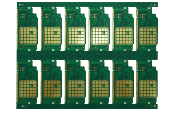
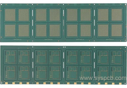
PCB Panelization refers to the process of connecting two or more PCB units together to form a larger PCB panel, offering various applications and advantages.
PCB Panelization advantages
Firstly, PCB panelization significantly improves the production efficiency of SMT processing.
By processing multiple PCB units into one large panel at once, the number of board transfers and cycle frequencies can be reduced, enabling the production of more circuit boards within the same timeframe and enhancing overall production efficiency. This is particularly important for manufacturers engaged in high-volume electronic product production.
Secondly, PCB panelization maximizes material utilization, thereby reducing costs.
By arranging small or irregularly shaped PCB units together on a panel, the usable area of the CCL substrate is fully utilized, minimizing waste and lowering manufacturing costs. This is a key consideration for PCB production processes focused on cost-effectiveness.
Furthermore, PCB panelization helps reduce production complexity and improves product yield.
By simplifying complex PCB structures into more manageable layouts, the technical challenges during production are minimized, leading to improved manufacturing quality and higher yield rates. This is equally crucial for ensuring product quality and enhancing production efficiency.
Factors to be considered during panelization
During the design phase of PCB panelization, multiple factors must be comprehensively considered. Beyond fundamental considerations, other detailed aspects need attention to ensure the final design meets product requirements.
First, a deeper analysis of product characteristics is required.
Including precise evaluation of circuit layout, signal transmission, and power consumption. This helps avoid interference and performance degradation caused by complex circuit structures, ensuring the stability and reliability of the entire panelized system.
Additionally, a balance between material utilization and production efficiency requires thorough optimization.
When determining the number and arrangement of panels, factors such as production line capacity and efficiency must be considered to avoid introducing unnecessary manufacturing bottlenecks. Careful layout and design can also minimize waste, contributing positively to environmental sustainability.
Regarding product reliability and performance, special attention must be paid to the impact of panelization on circuit stability and signal integrity. Proper layout can prevent signal line cross-talk and interference, thereby preserving circuit performance.
For high-frequency circuits and sensitive components, meticulous analysis and layout are even more critical to ensure stable and reliable operation under various working conditions.
Moreover, considerations of SMT production difficulty and manufacturing costs are paramount.
The panelization should align with SMT production processes to avoid introducing unnecessary technical challenges. A comprehensive evaluation of manufacturing costs—including material, labor, and equipment expenses—is essential to ensure the panelization is cost-effective.
Throughout the PCB panelization process, close collaboration with production lines is vital to ensure the design meets both product requirements and manufacturability.
PCB panelization Conclusion
In summary, PCB panelization design is a complex and multifaceted process that requires engineers to consider various aspects comprehensively. Through thoughtful design, not only can production efficiency be enhanced and costs reduced, but product reliability and performance can also be optimized.
In today’s rapidly advancing PCB assembly technology and manufacturing landscape, optimized PCB panelization continues to play a crucial role in driving the electronics manufacturing industry to higher levels of excellence.