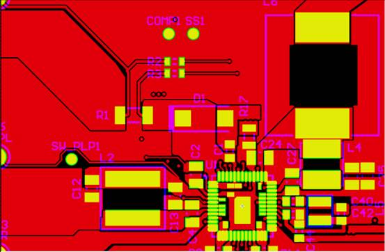
Copper laying in PCB design is a very important part of circuit board design. What is PCB copper laying, is to fill the unused space on the PCB with solid copper. The significance of laying copper is to reduce the impedance of the ground wire, improve the anti-interference ability; reduce the voltage drop, improve the efficiency of the power supply, connect to the ground wire, and reduce the loop area.
Table of Contents
The significance of PCB copper laying
The main benefit of laying copper is to reduce the impedance of the ground wire. (A large part of the so-called anti-interference is also caused by the reduction of the impedance of the ground wire). There are a lot of peak pulse currents in the digital circuit, so it is more necessary to reduce the impedance of the ground wire.
It is generally believed that for a circuit composed entirely of digital devices, a large area should be paved, while for an analog circuit, the ground loop formed by laying copper will cause electromagnetic coupling interference that is not worth the loss (except for high-frequency circuits). Therefore, not all circuits need to be covered with copper.
Advantages and disadvantages of PCB copper laying
First, Advantages of PCB copper laying
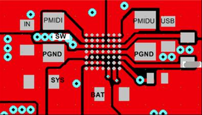
1. For EMC (electromagnetic compatibility) requirements, large areas of ground or power supply need to be covered with copper, which will play a shielding role, and some special grounds, such as PGND (protection ground), will play a protective role.
2. For PCB manufacturing requirements, generally in order to ensure the uniform effect of electroplating copper plating, or lamination without deformation and bending, copper is laid on PCB layers with less wiring.
3. For signal integrity requirements, give high-frequency digital signals a complete return path and reduce the wiring of the DC network. Of course, there are also reasons for heat dissipation, special device installation requires copper laying, and so on.
Second, Disadvantages of PCB copper laying
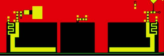
1. If the component pins are fully covered with copper, it may cause excessive heat dissipation, resulting in difficulties in desoldering and repair. So sometimes in order to avoid this situation, a cross connection is used for components (pin contact and pad contact are “+”).
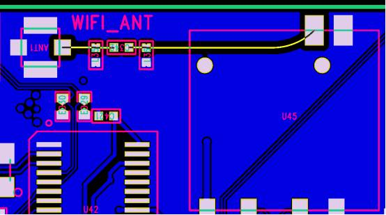
2. Placing copper in the area around the antenna will easily lead to weak signals, and the collected signal will be interfered. The impedance of copper paving will affect the performance of the amplifier circuit. Therefore, the area around the antenna part is generally not covered with copper.
The shape of PCB copper
solid shape copper
The solid copper clad has the dual functions of increasing the current and shielding. However, if the solid copper clad is subjected to wave soldering, there is a certain tension of thermal expansion and contraction, and the board may warp or even bubble. Therefore, for solid copper plating, several slots are generally opened to relieve the tension and cause the copper foil to blister.
grid shape copper
The grid is coated with copper, which mainly plays a shielding role, and the effect of increasing the current will be reduced. From the perspective of heat dissipation, grid copper not only reduces the heating surface of copper, but also plays a certain role in electromagnetic shielding. However, the production process has certain requirements on the shape of the grid, and the grid is too small to affect the quality and yield.
Design of PCB copper laying
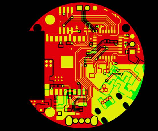
In PCB design, generally, each surface of the PCB should be covered with copper and grounded. The main reason is to prevent PCB bending deformation and various signal interference and crosstalk.
Therefore, copper should be grounded when wiring. However, since there are a large number of components and traces on the outer layer, the copper foil will be divided into many small isolated copper and slender copper skins by these component pads and their traces.
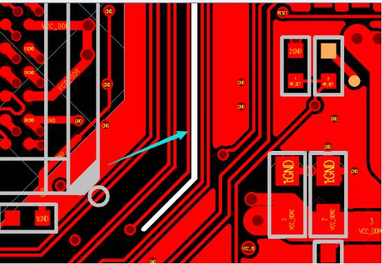
1. Handling broken copper
Those thin, long and poorly grounded ground copper will have an antenna effect, which will cause poor EMC problems. Therefore, it is necessary to avoid causing broken copper when pouring copper as much as possible. If it causes broken copper, it can be deleted.
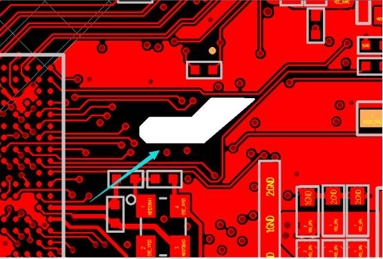
2. Handling Isolated Copper
Island(dead zone)copper problem, if the isolated copper is relatively small and equal to broken copper, it can be deleted. If it is very large, it can be defined as a certain ground to add vias, and there will be no isolated copper at this time.
PADS light painting file copper clad
The file designed by PADS needs to be paved again when it is opened for the second time. The reason is that the copper paving of PADS software is a linear copper skin, which is also the characteristic of PADS software. The amount of data on the linear copper sheet is large. If you close the software and reopen the saved copper layer, the file will be very slow and stuck. Therefore, after the PADS software is closed, only the copper skin frame of the design file is retained.
PADS copper laying method:
1. Fill (hatch)
Filling is to restore the copper filling, because the PADS software does not retain the entire designed copper skin, only the outer frame of the copper skin, so the second opening of the design file needs to restore the copper filling.
2. Perfusion (flood)
Copper filling is used for the first time after the PCB Layout is completed, or the PCB has changes (such as design rules) and copper filling needs to be used again.
3. Flat Links
The plane connection refers to the copper skin of the inner layer. The reason is that the copper skin designed by the PADS software only retains the outer frame of the copper skin. When the copper skin of the inner layer of the design file is opened for the second time, the plane connection needs to be selected to restore the copper laying.
Therefore, when the PADS design file is output to the Gerber file, the second time the design file is opened, it needs to be refilled to restore the copper filling. If the board factory helps the design engineer output Gerber, it needs to restore the copper filling operation, otherwise the output Gerber file lacks copper skin, resulting in manufacturing errors and the product cannot be used.
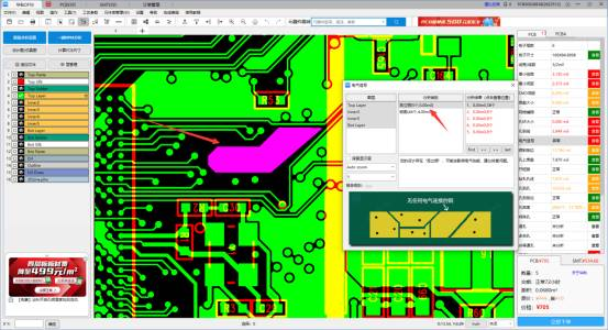
DFM check design copper laying
Regarding the manufacturability of broken copper and isolated copper, broken copper will be etched away due to the slender features during the manufacturing process, which will cause copper to separate, and fall off in other positions to cause short circuits in different networks.
When the CAM engineer of the board factory processes the production documents for isolated copper, he will inquire and confirm with the design engineer, because the isolated copper without network connection is an abnormal design. Therefore, the existence of isolated copper in the design will waste communication costs and delay the production cycle.
Get your exclusive quote immediately: fill out the form or send an email directly, and we will provide you with a quote service within 24 hours. Enjoy free DFM optimization and a 10% discount on SMT patches for your first order!