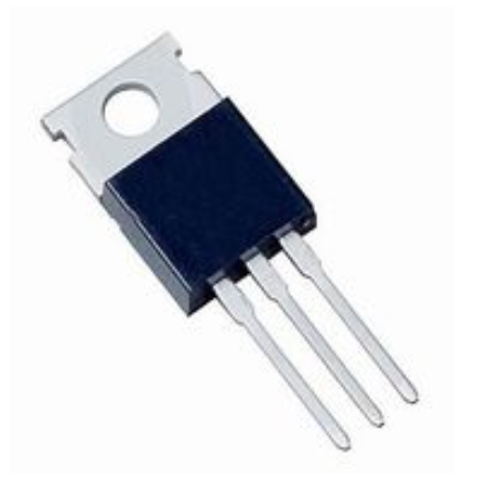
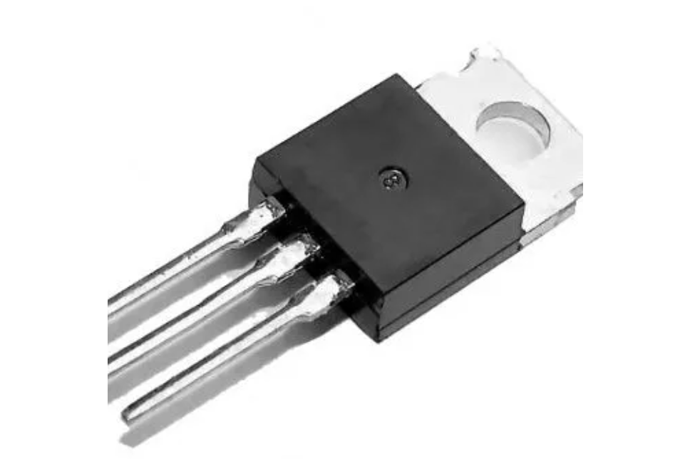
Field Effect Transistor (FET) is a semiconductor device that controls the magnitude of current through the electric field effect. It is widely used in electronic circuits such as amplifiers, switches, and impedance matching. The following provides a detailed introduction from the aspects of working principle, structural classification, characteristics, and application scenarios:
Table of Contents
1、 Working principle
The core principle of field-effect transistors is to use an electric field to regulate the concentration and movement of charge carriers (electrons or holes) in semiconductor materials, thereby controlling the conduction and cutoff of current.
-The basic structure includes three electrodes:
-Gate (G): Apply voltage to generate an electric field and control current.
-Source (S): The input terminal of charge carriers.
-Drain (D): The output terminal of charge carriers.
-During operation, the gate voltage will change the width or conductivity of the “conductive channel” in semiconductor materials (such as silicon):
-When the gate voltage reaches a specific threshold, the channel conducts, allowing current to flow from the source to the drain;
-When the gate voltage is insufficient, the channel is closed and the current is blocked.
2、 Main categories
Field effect transistors are mainly divided into the following two categories based on their structure and working principle:
1. Junction Field Effect Transistor (JFET)
-Structural features: Utilizing the reverse bias of the PN junction to control the channel current.
-It is divided into two types: N-channel and P-channel, with the difference being the doping type of the semiconductor material (N-type containing free electrons, P-type containing holes).
-Job characteristics:
-The gate needs to be biased in reverse (negative voltage applied to the N-channel and positive voltage applied to the P-channel) to deplete the carriers in the channel and control the current.
-There is no insulation layer, and the gate and channel are directly coupled through a PN junction, resulting in a small amount of current (reverse leakage current).
2. Insulated Gate Field Effect Transistor (MOSFET, Metal Oxide Semiconductor FET)
-Structural features: There is a layer of insulating oxide (such as SiO ₂) between the gate and the channel, which isolates the gate from the semiconductor, resulting in almost zero gate current (insulating properties).
-Divided into enhanced and depleted types, the difference lies in whether the channel exists at zero gate voltage:
-Enhanced MOSFET: When the gate voltage is zero, the channel does not conduct, and a gate voltage needs to be applied to “enhance” the channel conductivity (such as common NMOS and PMOS).
-Depletion MOSFET: When the gate voltage is zero, the channel is already conducting, and a reverse gate voltage needs to be applied to “deplete” the carriers to block the current (less commonly used).
-Application advantages:
-The input impedance is extremely high (up to 10 ¹² Ω or more), almost consumes no current, and is suitable for high-frequency circuits and large-scale integrated circuits (such as CPUs and memory chips).
3、 Core Features
| Characteristics | Description |
| Voltage control | Current is controlled by gate voltage (voltage type devices) rather than current control (compared to bipolar junction transistors). |
| High input impedance | The gate current is extremely small (MOSFET is almost zero), which has little impact on the front-end circuit and is suitable for multi-stage amplification. |
| Good thermal stability | Temperature sensitivity lower than bipolar transistors, less prone to performance fluctuations due to temperature drift. |
| Easy to integrate | Simple structure, suitable for large-scale manufacturing, is the foundation of CMOS (Complementary Metal Oxide Semiconductor) technology. |
| Low power consumption | Extremely low static power consumption, especially suitable for battery powered devices such as mobile phones and laptops. |
4、 Application scenarios
1. Switching elements in electronic circuits
-Such as computer memory (RAM), logic gate circuits (NAND gates, NOR gates, etc.), utilizing the on/off characteristics of MOSFETs to achieve binary signal processing.
2. Power amplification and power management
-Power MOSFETs are used in electric vehicles, power adapters, inverters, etc. to control high current on/off, with high efficiency and low losses.
3. Signal amplification
-Utilize the voltage amplification characteristics of JFET or MOSFET in RF circuits (such as mobile phone antenna modules) and audio amplifiers.
4. Sensors and Special Devices
-Such as pressure sensors (using gate voltage to respond to mechanical stress) and biochips (detecting changes in ion concentration).
5、 Comparison with Bipolar Transistor (BJT)
| Characteristics | Field Effect Transistor (FET) | Bipolar Transistor (BJT) |
| Control mode | Voltage control (gate voltage regulates current) | Current control (base current regulates collector current) |
| Input impedance | High (MOSFET can reach 10 ¹² Ω) | Low (about 10 ³ Ω) |
| Thermal stability | good | poor (prone to thermal breakdown) |
| Noise characteristics | Low (especially suitable for high-frequency circuits) | High |
| Manufacturing process | Simple, suitable for large-scale integration | More complex |
6、 Development and Frontiers
-Nanotechnology applications: With the advancement of semiconductor processes, MOSFET sizes have been reduced to the nanometer level (such as 3nm process chips), improving integration and speed.
-New structural devices, such as FinFET (FinFET) and GAAFET (Fully Surrounding Gate Transistor), optimize electric field control through three-dimensional structure to solve short channel effect (leakage problem).
-Wide bandgap semiconductors, such as silicon carbide (SiC) MOSFETs and gallium nitride (GaN) FETs, are suitable for high-voltage and high-frequency scenarios, such as new energy vehicles and 5G base stations.
Field effect transistors have become the cornerstone of modern electronics industry due to their high efficiency, low power consumption, and ease of integration, driving revolutionary development in fields such as computers, communications, and energy.
Get your exclusive quote immediately: fill out the form or send an email directly.As a professional PCB manufacturer for hobbyist , we will provide you with a quote service within 24 hours. Enjoy free DFM optimization and a 10% discount on SMT patches for your first order!