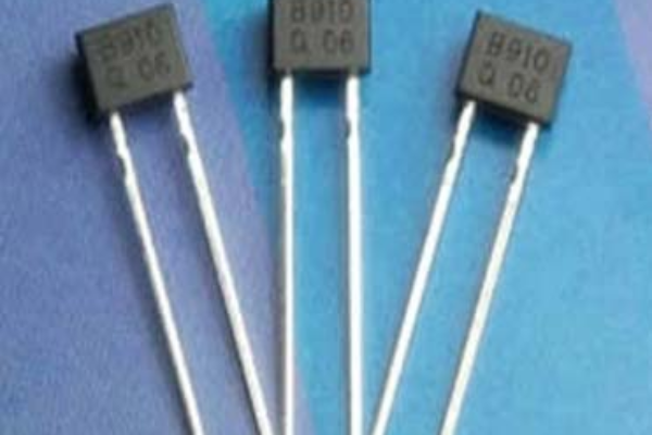
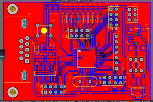
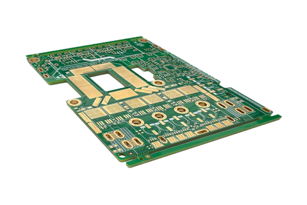
The surface mount technology (SMT) conforms to the trend of miniaturization and light weight of electronic products, and lays a foundation for realizing the light, thin, short and small electronic products.
After the SMT technology entered the 1990s, it has reached a mature stage. However, with the rapid development of electronic products in the direction of portable, miniaturization,networking and multimedia, higher requirements for electronic assembly technology have been put forward, and new high-density assembly technology are emerging, among them, BGA (Ball Grid Array) is a high-density assembly technology that has entered the practical stage.
The BGA technology research began in the 1960s and was first adopted by IBM in the United States, but it was not until the early 1990s that the BGA really entered the practical stage.
In the 1980s, higher demands were placed on the miniaturization of electronic circuits and the number of I/O leads. In order to meet this requirement, the pin pitch of QFP has now grown from 1.27mm to 0.3mm. As the pitch of the pins continues to shrink, the number of I/O pins continues to increase, and the package size continues to increase, which brings many difficulties to the assembly and production of the circuit, resulting in a decrease in yield and an increase in assembly costs. On the other hand, due to manufacturing technology limitations such as components lead frame processing accuracy, 0.3mm is the limit of QFP pin pitch, which limits the increase in assembly density.
Therefore, an advanced chip package BGA (Ball Grid Array) came into being, its I/O terminals in the form of a circular or columnar dot array distributed under the package. The lead pitch is large and the lead length is short, so that the BGA eliminates the problem of coplanarity and warpage caused by the leads in the fine pitch components. The advantage of BGA technology is that it can increase the I/O number and spacing, eliminating the production cost and reliability problems caused by the high I/O number of QFP technology.
The industrial department of JEDEC (Joint Electronic Device Engineering Council) (JC-11) has developed the physical standard for BGA packages. The biggest advantage of BGA compared with QFP is that the I/O lead pitch is large, and the registered lead pitch is 1.0mm, 1.27mm and 1.5mm, and it is currently recommended to replace the 0.4mm-0.5mm fine pitch device with a 1.27mm and 1.5mm pitch BGA.
The structure of BGA devices can be divided into two types according to the shape of solder joints: ball solder joints and columnar solder joints. The ball joints include CGBA (Ceramic Ball Grid Array), TBGA (Tape Automatic Ball Grid Array) and PBGA (Plastic Ball Grid Array). CBGA, TBGA, and PBGA are divided by package method. The columnar solder joint is called CCGA (Ceramic Column Grid Array).
The advent of BGA technology is a major advancement in IC devices from quadrilateral lead to array solder joint packaging, which enables smaller devices, more leads, and superior electrical performance, as well as performance advantages over conventional assembly techniques. These performance advantages include high-density I/O interfaces, good thermal dissipation, and the ability to make small components with high clock frequencies.
Because the BGA device has a relatively large spacing, it has the ability to automatically align and position during reflow soldering, so it is easier to operate than other similar components, such as QFP, and has high reliability during assembly. According to some foreign printed circuit board manufacturing technical data, BGA devices can consistently achieve defect rate less than 20PPM (Parts Per Million) when using conventional SMT process specifications and equipment for assembly and production. Corresponding devices, such as QFP, have a product defect rate of at least 10 times greater during assembly.
In summary, the performance and assembly of BGA devices is superior to conventional components, but many manufacturers are still reluctant to invest in the ability to mass produce BGA devices. The main reason is that the testing of solder joints of BGA devices is quite difficult, and it is not easy to guarantee the quality and reliability.


