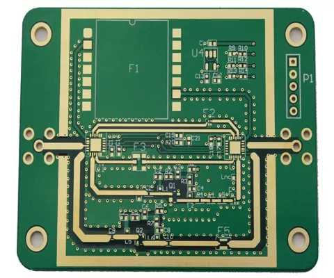
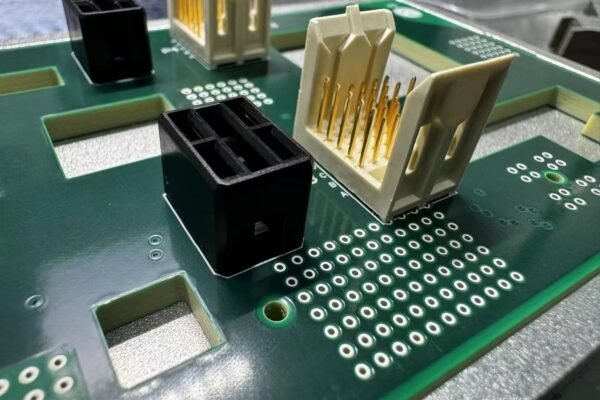
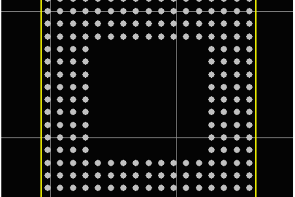
In the ever-evolving world of electronics, Printed Circuit Board (PCB) design plays a crucial role in ensuring the optimal performance of devices. One of the most critical aspects of modern PCB design is impedance control. This article delves deep into the concept of Impedance Control PCB, exploring its significance, techniques, benefits, and applications in today’s high-speed and high-frequency electronic systems.

Table of Contents
Understanding Impedance Control in PCB Design
Impedance control in PCB design refers to the deliberate management of the electrical impedance of traces on the circuit board. This process is crucial for maintaining signal integrity, especially in high-frequency and high-speed applications.
What is Impedance?
Impedance, in the context of PCBs, is the opposition that a circuit presents to the flow of electrical signals. It’s a complex quantity that includes both resistance and reactance.
Why is Impedance Control Important?
Impedance control is vital for several reasons:
It prevents signal distortion and reflection
It ensures reliable communication between electronic components
It maintains signal integrity in high-frequency applications
It reduces electromagnetic interference (EMI)

Techniques for Implementing Impedance Control in PCBs
Achieving effective impedance control requires careful consideration of various factors and the implementation of specific techniques.
PCB Stack-up Design
The PCB stack-up is crucial for impedance control. It involves:
Selecting appropriate dielectric materials
Determining the number of layer
Defining the thickness of each layer
Trace Width and Spacing
The width of traces and their spacing from other conductive elements significantly affect impedance. Designers must carefully calculate and maintain these dimensions.
Dielectric Constant Consideration
The dielectric constant of the PCB material plays a vital role in impedance control. Materials with lower dielectric constants are often preferred for high-frequency applications.
Via Design and Placement
Proper via design and placement are essential for maintaining controlled impedance, especially in multilayer PCBs.
Benefits of Impedance Control in PCB Design
Implementing impedance control in PCB design offers numerous advantages:
Improved Signal Integrity
Controlled impedance ensures that signals maintain their quality as they travel through the PCB, reducing distortion and loss.
Enhanced High-Frequency Performance
For applications operating at high frequencies, impedance control is crucial for maintaining signal fidelity and preventing unwanted reflections.
Reduced Electromagnetic Interference (EMI)
Proper impedance control helps minimize EMI, both within the PCB and to external components.
Increased Reliability
By maintaining consistent signal quality, impedance-controlled PCBs contribute to the overall reliability of electronic systems.
Applications of Impedance Control PCBs
Impedance control is critical in various industries and applications:
Telecommunications
In telecommunications equipment, where signal integrity is paramount, impedance-controlled PCBs ensure clear and reliable data transmission.
Aerospace and Defense
The aerospace and defense sectors rely heavily on impedance-controlled PCBs for their high-performance, mission-critical systems.
High-Speed Computing
Modern computing systems, especially those dealing with high-speed data processing, benefit significantly from impedance control.
Medical Devices
Precision and reliability in medical devices are ensured through the use of impedance-controlled PCBs.
Challenges in Implementing Impedance Control
While the benefits of impedance control are clear, designers face several challenges:
Complexity in Design
Implementing effective impedance control can significantly increase the complexity of PCB design.
Cost Considerations
The materials and manufacturing processes required for impedance-controlled PCBs can be more expensive.
Balancing Performance and Manufacturability
Designers must strike a balance between achieving optimal impedance control and ensuring that the PCB can be manufactured efficiently.
Tools and Software for Impedance Control Design
Several tools and software packages are available to assist designers in implementing impedance control:
Electromagnetic Field Solvers
These tools help in accurately calculating and simulating impedance in complex PCB designs.
PCB Design Software with Impedance Control Features
Modern PCB design software often includes built-in features for impedance calculation and control.
Impedance Calculators
Specialized calculators help designers quickly determine the correct trace dimensions for desired impedance values.
Future Trends in Impedance Control PCB Design
As technology continues to advance, several trends are emerging in the field of impedance control PCB design:
Integration with AI and Machine Learning
AI and machine learning are being incorporated into PCB design tools to optimize impedance control automatically.
Advanced Materials
New PCB materials with improved dielectric properties are being developed, offering better impedance control capabilities.
3D Printing in PCB Manufacturing
The advent of 3D printing in PCB manufacturing may open new possibilities for implementing complex impedance control structures.
Conclusion
Impedance Control PCB design is a critical aspect of modern electronics, ensuring signal integrity and optimal performance in high-frequency and high-speed applications. By understanding and implementing proper impedance control techniques, designers can create more reliable, efficient, and high-performing electronic systems. As technology continues to advance, the importance of impedance control in PCB design will only grow, making it an essential skill for electronics engineers and PCB designers.
Frequently Asked Questions
1. Q: What is the primary purpose of impedance control in PCB design?
A: The primary purpose of impedance control in PCB design is to maintain signal integrity by managing the electrical impedance of traces, preventing signal distortion, reflection, and ensuring reliable communication between components, especially in high-frequency and high-speed applications.
2. Q: How does the PCB stack-up affect impedance control?
A: The PCB stack-up significantly affects impedance control by determining the dielectric thickness, material properties, and layer arrangement. These factors directly influence the impedance of traces and must be carefully designed to achieve the desired impedance values.
3. Q: What are some common challenges in implementing impedance control in PCBs?
A: Common challenges include increased design complexity, higher manufacturing costs, balancing performance with manufacturability, and the need for specialized knowledge and tools. Additionally, maintaining consistent impedance across different board areas and through vias can be challenging.
4. Q: How does impedance control contribute to reducing electromagnetic interference (EMI)?
A: Impedance control helps reduce EMI by minimizing signal reflections and maintaining consistent signal quality. This reduces the likelihood of signals radiating unwanted electromagnetic energy, which can interfere with other components or nearby devices.
5. Q: What industries benefit most from impedance-controlled PCBs?
A: Industries that benefit most from impedance-controlled PCBs include telecommunications, aerospace and defense, high-speed computing, medical devices, and any sector dealing with high-frequency or high-speed electronic systems where signal integrity is crucial.


