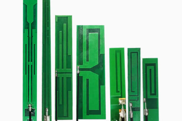
Generally there are four methods to do PCB outline, routing, punching, V-grooving, and Stamp holes. Normally V-groove and stamp holes only use as an auxiliary means of profile processing.
1. milling profile.
Use CNC miller to contour mill according to milling data and use the corresponding positioning hole to fix PCB to milling machine, the milling data provided by the programmers in CAM depart of PCB manufacturer, since the space between each printed circuit board is not big, usually about 3mm, so the milling bit is generally less than 3mm. First drill positioning holes in the base milling plate, then fix PCB and milling machine with a pin, and then milling outline using shape data.
2. Punching profile.
Use puncher to punching PCB shape, First make a mold, the positioning holes in mold and PCB positioning holes are at exactly same point. Generally choose around φ3.0mm hole to match the alignment.
3. V-groove.
Use of V-groove machine to cut along the PCB designed V-groove line. PCB panel will be cut into several parts connected to each other;
4. Stamp holes.
Drill holes at the connecting positions between PCB and board edge.
Milling is suit for those simple boards with simple outline, it normally no so much burrs like V-grooving and Stamp holes. If don’t make the tooling holes well, the boards may be easy moving while milling, which cause to the outline crooked.
If you need the outline more precision and nice, another way is to custom a tool for punching, in such way, the outline shape is very exact and no so much burr on the edge. It is used for those boards in big panel with small boards, special outline as well as high precision boards. Punching also can speed up the production lead time. But for such way the cost is expensive than routing.