In modern electronic manufacturing, PCBA (Printed Circuit Board Assembly) serves as the heart of electronic products, carrying the intelligent soul from consumer electronics to aerospace equipment. As a PCB enterprise, a deep understanding of PCBA manufacturing technology is not only the key to enhancing product added value, but also the core competitiveness to connect the entire electronic manufacturing chain. This article will systematically analyze the technical points and industry frontiers of the two core processes of SMT and DIP.
Table of Contents
1、 PCBA manufacturing processes Panorama
PCBA manufacturing is a systematic engineering process that converts bare boards into functional circuit components, and its manufacturing process mainly includes four major steps:
–SMT surface mount processing: Processing surface mount components (accounting for over 90% of modern components)
-DIP plug-in processing: for through-hole plug-in components (large connectors/transformers, etc.)
-PCBA testing: comprehensive verification covering electrical performance to environmental reliability
-Finished product assembly: shell integration and final packaging
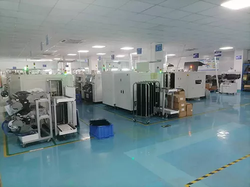
The advanced production line achieves full process digital control through MES system, and the overall equipment efficiency (OEE) can reach over 85%. It supports the daily processing of 20 different BOM versions of multi variety mixed production mode.
2、 SMT SMT SMT process: the pinnacle of precision manufacturing
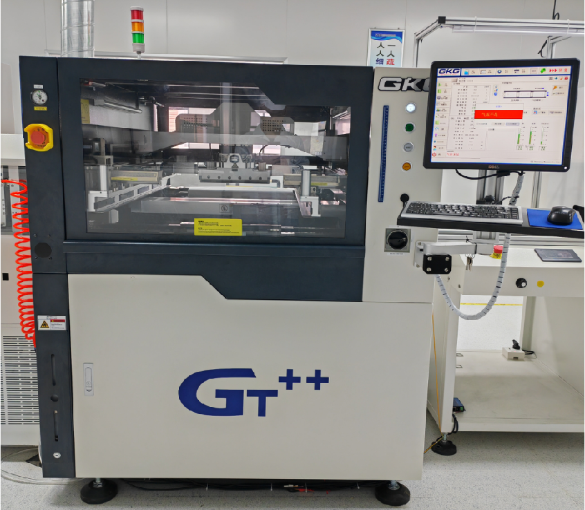
1. Solder Paste Printing: Micro scale Art
-Steel mesh positioning: laser cutting steel mesh opening and welding pad error ≤ 15 μ m
-Scraper control: The stainless steel scraper is pushed at a 60 ° angle, and the solder paste thickness is controlled at 100 ± 10 μ m
-SPI detection: Real time monitoring of volume accuracy of 0.01mm ³ by 3D optical system, intercepting 87% of welding defects in advance
2. Component mounting: the game between speed and accuracy
The high-speed surface mount machine achieves astonishing accuracy through multimodal alignment technology:
| Component type | Mounting accuracy | Mounting speed |
| 0201 resistor | ± 25 μ m | 240000 points/hour |
| QFP chip | ± 35 μ m | 80000 points/hour |
| 0.4mm pitch BGA | ± 15 μ m | Special nozzle treatment |
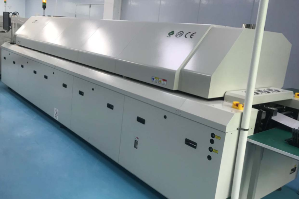
3. Reflow soldering: precise control of temperature curve
The ten temperature zone reflow soldering furnace ensures lead-free soldering quality through gradient temperature control:
| Preheating zone: room temperature → 150 ℃ (slope 2-4 ℃/s, 60~150s) Constant temperature zone: 150 → 200 ℃ (slope<1 ℃/s, 60~120 seconds) Reflux zone: peak temperature 235~245 ℃ (30~40s, solder paste completely liquefied) Cooling zone:>4 ℃/s cooling rate (to avoid thermal stress damage) |
The nitrogen protection environment reduces the porosity of solder joints from 15% to below 3%.
3、 DIP plugin process: intelligent upgrade of traditional skills
1. Three major innovations in precision insertion and installation
-Pre forming processing: Automatic bulk capacitor trimming machine ensures that the horizontal width tolerance of the pins is less than 5%
-Robot plugin: Six axis robotic arm with machine vision, pin insertion success rate>99.97%
-Selective wave soldering: local soldering temperature control ± 2 ℃ to avoid damage to heat sensitive components
2. Key parameters of wave soldering
| Flux spraying: Foam spraying with a thickness of 10-20 μ m Preheating temperature: 110-130 ℃ (to reduce thermal shock) Soldering temperature: 250 ± 5 ℃ (Sn99.3Cu0.7 alloy) Contact time: 3-5 seconds (pin immersion depth ≥ 2/3) |
The post weld automatic optical inspection (AOI) system scans the through-hole filling rate at a speed of 0.05 seconds per point.
4、 Quality Fortress: Testing and Verification System
1. Four dimensional detection technology matrix
| Detection method | Detection capability | Defect capture rate |
| 3D SPI | Solder Paste Volume/Shape | >95% |
| AOI | Offset/Missing Parts/Polarity | 98% |
| X-ray | BGA cavity/virtual soldering | 99.5% |
| FCT Test | Functional Abnormality | 100% |
2. Reliability verification in extreme environments
-Temperature cycle: -40 ℃~125 ℃ 1000 cycles (simulated for 10 years of use)
-Vibration test: 20~2000Hz sweep frequency (required for automotive electronics)
-Three proof coating: Polyurethane coating makes the insulation impedance>10 ¹² Ω
5、 Green Intelligent Manufacturing: A Technological Path for Sustainable Development
Modern PCBA factories achieve green production through triple environmental protection technology:
-Waste gas treatment: Three stage catalytic combustion controls VOCs below 20mg/m ³
-Wastewater reuse: RO reverse osmosis achieves a heavy metal removal rate of 99.97%
-Hazardous waste recycling: The utilization rate of waste tin slag resources exceeds 95%
The GB/T 39560 testing standard implemented in 2025 is fully aligned with the international IEC 62321, strengthening the control of ten types of hazardous substances.
Future Factory: The Technological Revolution of PCBA 4.0
Heterogeneous integration technology is breaking through traditional process boundaries:
-Buried resistance and capacitance: embedding passive components between PCB layers to reduce surface mount
-Flip Chip Soldering: Flip Chip technology achieves a 40 μ m bump spacing
-Laser induced Interconnection: Direct Writing of Micro scale Circuits Using LIFT Technology
The flexible manufacturing system reduces the preparation time of testing fixtures by 60% through modular fixtures, supports ICT/FCT free switching, and even for small batch orders of 50 pieces, the laser steel mesh production cycle is compressed from 24 hours to 2 hours.
The innovation of PCBA manufacturing technology continues to drive the evolution of the electronics industry, from smartphones to satellite communication devices. When the 01005 packaged component (0.4 × 0.2mm) is precisely mounted through a 12 μ m nozzle, and when the 1000 pin BGA presents a perfect solder joint contour under X-ray, behind these microscopic miracles is the triple synergy of materials science, precision machinery, and digital intelligence.
As a PCB company, breaking down the process barriers between SMT and DIP means not only providing bare boards, but also delivering plug and play intelligent modules – this will be a key springboard for the industry value chain transition. The future belongs to the creators who turn circuit boards into intelligent carriers.