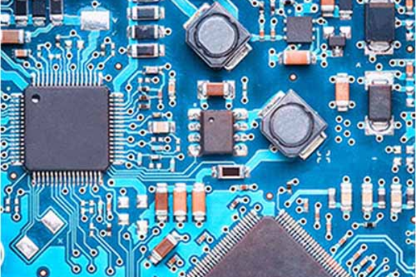
In the miniaturization of electronic products, Surface Mount Technology (SMT) is like a precision high-speed train, carrying the core circuit manufacturing mission from smartphones to aerospace equipment. As a new generation of electronic assembly technology that replaces traditional through-hole welding, SMT production lines have achieved a breakthrough in electronic products in terms of volume, performance, and reliability by accurately attaching micro components to the surface of PCBs.
Table of Contents
1、 The core architecture of SMT production line
A complete SMT production line is a combination of automation and precision control, with its core equipment working together to complete the entire process from solder paste printing to solder solidification:
1. Printing unit: Micron level control of solder paste
-Solder Paste Printing Machine: The solder paste is accurately missed onto the PCB pads through a steel mesh template, with an accuracy of ± 0.025mm. The fully automatic model can be connected to front and rear equipment to achieve high-speed printing of over 300 pieces per hour.
-Solder paste mixing and reheating machine: Ensure stable viscosity of solder paste and avoid cold soldering or collapse defects.
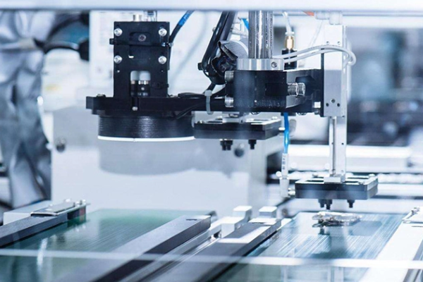
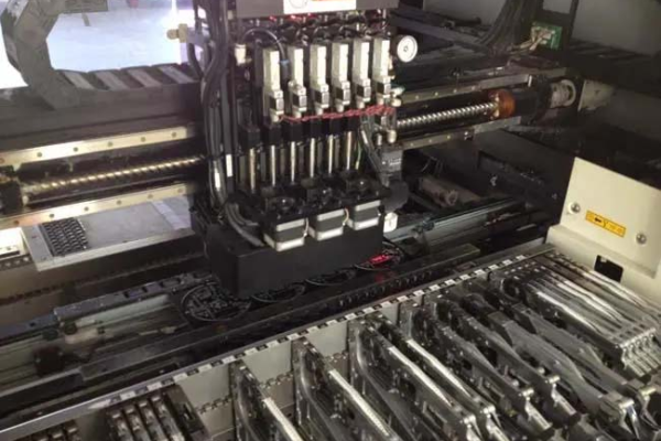
2. Mounting Unit: Peak of Speed and Accuracy
-SMT machine: the “heart” of the production line, accounting for over 70% of the total investment. By using a vacuum suction nozzle to extract components and combining with a visual positioning system to achieve a mounting accuracy of ± 0.05mm, high-speed models can reach 250000 points per hour (CPH).
-Dual unit strategy: high-speed machine mounted resistors and capacitors+multifunctional machine processing IC/BGA, efficiency increased by 40%.
3. Welding and Testing Unit: Quality Closed Loop Control
-Reflow soldering furnace: adopts a four temperature zone curve (preheating → insulation → reflow → cooling), with a temperature control accuracy of ± 2 ℃, to uniformly melt the solder and form a reliable connection.
-Testing equipment matrix:
-SPI (Solder Paste Tester): 3D scans the thickness and shape of solder paste to prevent offset and low tin content
-AOI (Automatic Optical Inspection): Based on AI image analysis of solder joint defects, the detection rate is greater than 99.5%
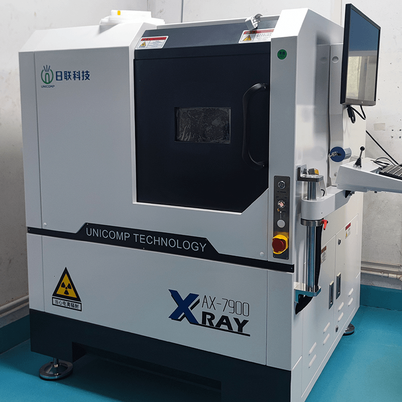
–X-RAY: Penetrating the internal voids of BGA/CSP solder balls to solve hidden defects
4. Logistics and auxiliary systems
-Boarding/Connecting/Unloading Machine: Achieve automatic flow of PCBs between devices, reducing manual intervention
-Repair workstation: precise repair for defects detected by AOI or X-RAY
>Example of device type comparison
| Equipment type | Semi automatic line configuration | Fully automatic line configuration |
| Printing machine | Semi automatic (requiring manual board transfer) | Fully automatic+SPI online monitoring |
| Surface mount machine | Single multifunctional machine | High speed machine+multifunctional machine online |
| Detection System | Manual Visual Sampling | AOI+X-RAY Full Inspection |
| Logistics System | Manual Handling | Automatic Transfer Platform+Intelligent Warehousing |
—
2、 SMT standardized process flow
The Nine Step Rule of Precision Manufacturing
1. Solder paste printing: The accuracy of steel mesh opening determines the reliability of solder joints, and a laser cutting template is required for a spacing of 0.5mm
2. SPI detection: Real time feedback of printing defects, adjustment of scraper pressure and speed
3. Component mounting: First, attach small-sized resistors and capacitors (0402/0201), then attach precision ICs such as QFP/BGA
4. Reflow soldering: Temperature curve is the core – heating slope ≤ 2 ℃/s, peak temperature 245 ± 5 ℃
5. AOI initial inspection: Confirm the welding quality of the first piece, capture the standing monument, offset, and tin bead
6. Plug in soldering (mixed board): through-hole components are soldered twice through wave soldering
7. Three proof coating: spraying nano coating for moisture and corrosion prevention
8. X-RAY inspection: BGA solder joint void rate requirement<15%
9. Board splitting test: To avoid stress damage, a rotary cutting board splitting machine is used instead of manual board breaking
3、 The revolutionary advantages of SMT technology
Compared to traditional through hole insertion (THT), SMT brings five major dimensional upgrades:
-Miniaturization: Component volume reduced by 80%, PCB area reduced by 40-60%
-High frequency performance: Short pin design reduces parasitic inductance and supports high-speed signals above 3GHz
-Reliability leap: solder joint defect rate<0.01 ‰ (THT is 0.1 ‰), vibration resistance increased by 3 times
-Cost optimization: Material waste reduced by 30%, labor dependence reduced by 50%
-Green manufacturing: no cleaning solder+nitrogen reflow soldering, reducing VOC emissions by 90%
4、 The technological defense line of quality control
On the micron scale battlefield, three major technologies build zero defect barriers:
1. Data traceability system: MES platform binds the process parameters of each PCB (such as printing pressure, reflow temperature zone value)
2. AI prediction model: predict reflow solder joint deformation based on SPI solder paste thickness, and adjust the temperature curve in advance
3. Analysis of CPK process capability: Key indicators such as patch position offset CPK ≥ 1.33
>Case warning: A car camera factory did not use SPI, resulting in uneven thickness of solder paste in batches, with a defect rate of 12% after reflow. After introducing full inspection SPI, the defect rate decreased to 0.3%.
5、 Future trend: evolving towards smart factories
-Digital twin: Virtual simulation optimizes patch path, reducing real machine debugging time by 50%
-Flexible production line: Modular equipment supports “one click switching” of product types, with a switching time of less than 10 minutes
-IIoT integration: Real time upload of welding temperature, mounting accuracy and other data to the cloud, generating device health reports
Conclusion: The neural center of precision manufacturing
The SMT production line has evolved beyond simple assembly tools into a super manufacturing system that integrates precision machinery, optical recognition, materials science, and artificial intelligence. When a PCB the size of a fingernail carries billion level transistors, it is the 30000 rpm surface mount machine spindle, ± 2 ℃ temperature controlled reflow soldering furnace, and 0.4 μ m resolution AOI lens that together hold up the microscopic miracle of modern electronics industry.
>Intel Manufacturing Director Sophia Coleman’s assertion:
>Chips are the brains of electronics, while SMT production lines are the creators who give them bodies. ”
As an irreplaceable cornerstone technology in the field of electronic manufacturing, SMT will continue to drive the evolution of electronic products towards smaller, faster, and more reliable directions – this is an endless precision revolution.