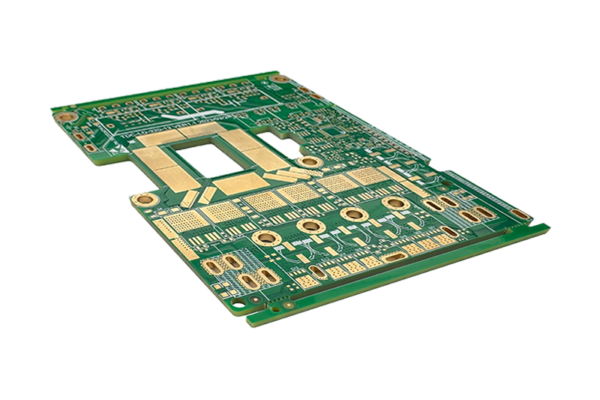
The simple description of the tin board is the circuit board that has been sprayed with tin. It is easier to understand that the board is immersed in the molten solder spray during the PCB processing process, so that the surface of the copper on the PCB surface is covered with a layer of solder, and then the excess tin on the PCB is removed by hot-air cutter and other processing techniques to ensure that the appearance and other quality requirements are met.
HASL PCB
In the actual PCBA processing, because the solder paste used is the same substance for soldering in the circuit board and SMT chip processing, plug-in processing and other process, it is possible to get just the right soldering effect, such as soldering reliability and soldering strength. Let’s give you a brief analysis of the advantages and disadvantages of using hot air solder leveling in PCBA SMT process.
I. Advantages of hot air solder leveling:
It can prevent the exposed copper surface from being corroded or oxidized.
The wettability is better during the soldering process of the components, and the soldering is easier.
II. Disadvantages of hot air solder leveling:
The high thermal stress during processing may damage the PCB board and cause blemishes or defects.
The flatness at the vertical level is poor, and it is not suitable for the soldering and use of fine pitch components. The flatness can be improved by increasing the horizontal level.
It is not suitable for soldering pins with fine pitch and components that are too small, because the surface flatness of the HASL is poor. In PCBA processing, tin bead is easy to occur, and it is easy to cause short circuit to the fine pitch components.


