Why electromagnetic wave scanning in PCBs?
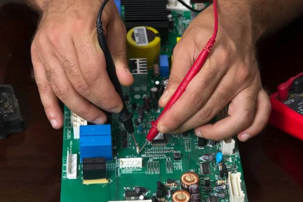
Circuits that carry rapidly changing electrical currents can generate unwanted electromagnetic waves, wasting energy, causing interference with other electronic equipment, and potentially posing health risks to users. To ensure that such emissions are within acceptable limits, electronic products such as mobile phones and laptops must undergo tests for this electronic smog before they can be marketed. Those tests have traditionally been done in large rooms designed to capture all the electromagnetic waves emitted from the device.
What is the method of electromagnetic wave scanning?
An alternative to this costly process involves scanning the electromagnetic printed circuit board field very close to the devices circuit boards (the near field), and then calculating the resulting radiation at a distance (the far field). But those calculations can take powerful computers many hours to complete electronic. The mathematical model developed by Zhao and co-workers translates near-field measurements into an accurate estimate printed circuit board of far-field radiation in less than 10 minutes on a standard desktop computer printed circuit board. Our simulation technique could help to shorten the product design cycle, save laboratory space, and reduce product development cost, says Zhao.
Implementation method
The researchers model mathematically printed circuit board mimics the readings from a scan of the near-field above a printed circuit board. Their simulation relies on a series of virtual magnetic dipoles effectively tiny, imaginary bar magnets electronic that collectively replicate the variations in the measured magnetic field printed circuit board. The simulation runs iteratively, each time altering the magnetic dipoles so that they fit the data better. This process of differential evolution eventually produces a solution that is a sufficiently close match to the circuit-boards near field. Printed circuit board the researchers then use those magnetic dipoles to simplify their calculation of the far-field radiation produced by the device printed circuit board.
The researchers tested their model using simulated near-field data from a thin, L-shaped metal strip laid on a small circuit board. The data contained 1,273 sample points, each 10 millimeters above the board. The model could approximate this magnetic field using just a few virtual magnetic dipoles.
Printed circuit board the match improved as they added more dipoles, until they reached very good agreement at nine dipoles adding a tenth did not significantly improve the match printed circuit board. The team is now working to refine the system to make it suitable for use by the electronics industry.