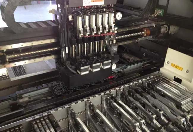
Surface Mount Technology (SMT) is a widely used PCB assembly process where electronic components are mounted directly onto the surface of a printed circuit board (PCB). However, in some cases, designers and manufacturers notice that certain plated through-holes (PTHs) lose conductivity after the SMT process. This issue can lead to functional failures and connectivity problems in the final product. In this article, we explore the reasons behind non-conductive holes after SMT and how to prevent such issues in PCB manufacturing.
Table of Contents
1. What are the reasons for non-conductive holes appearing after SMT?
1.1 High Reflow Temperature Impact on Plated Holes
During the SMT process, PCBs go through a high-temperature reflow soldering process, typically reaching 230°C–260°C.
Extreme heat can cause thermal expansion, leading to barrel cracking or plating separation, disrupting electrical continuity.
Materials with high coefficient of thermal expansion (CTE) are more prone to these failures.
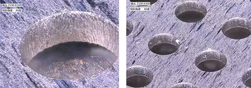
1.2 Poor Via Plating Quality
The integrity of via plating is crucial for maintaining electrical conductivity.
If the copper plating inside the via is too thin or contains voids, cracks may form due to thermal stress.
Contaminants or improper electroplating processes can result in poor adhesion between copper layers, leading to delamination after multiple heat cycles.
1.3 Solder Mask or Flux Contamination
Excess solder mask or solder paste residue may enter the vias, causing electrical insulation.
Flux residues from the reflow process can remain inside the hole, preventing proper electrical contact.
Improper cleaning after soldering can leave unwanted residues that reduce conductivity.
1.4 PCB Warpage and Mechanical Stress
PCBs may warp during the high-temperature SMT process, putting mechanical stress on plated through-holes.
Excessive warpage can lead to micro-cracks in the copper plating, causing intermittent or complete loss of conductivity.
2. How to Prevent Non-Conductive Holes After SMT?
2.1 Optimize PCB Material Selection
Use materials with low CTE to minimize expansion-related plating failures.
High-Tg (glass transition temperature) laminates provide better thermal stability.
2.2 Improve Plating Process Quality
Ensure proper copper thickness in plated through-holes (typically 18-25μm for standard PCBs).
Implement thorough via wall cleaning before electroplating to prevent voids and adhesion failures.
2.3 Control Reflow Soldering Parameters
Optimize reflow profiles to reduce excessive thermal stress on vias.
Implement gradual heating and cooling cycles to avoid sudden thermal expansion.
2.4 Design Considerations for Vias
Use teardrop pads around vias to reduce stress concentration.
Consider via-in-pad designs with proper filling and capping to prevent solder mask contamination.
Avoid placing critical vias in areas with high thermal or mechanical stress.
2.5 Post-SMT Inspection and Testing
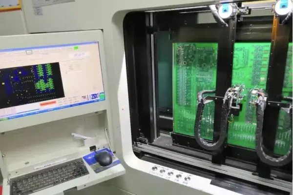
Conduct X-ray inspection to detect via cracks or voids after reflow.
Perform electrical continuity testing to verify via conductivity.
Implement thermal cycling tests to evaluate PCB durability under operating conditions.
Conclusion
Non-conductive holes after SMT can result from thermal expansion, poor via plating, solder mask contamination, or mechanical stress. To prevent these issues, manufacturers should optimize material selection, plating processes, reflow conditions, and PCB design. By implementing strict quality control measures and thorough post-SMT testing, PCB reliability and performance can be significantly improved, reducing the risk of electrical failures in electronic devices.
Get your exclusive quote immediately: fill out the form or send an email directly.As a professional PCB manufacturer for hobbyist , we will provide you with a quote service within 24 hours. Enjoy free DFM optimization and a 10% discount on SMT patches for your first order!