Table of Contents
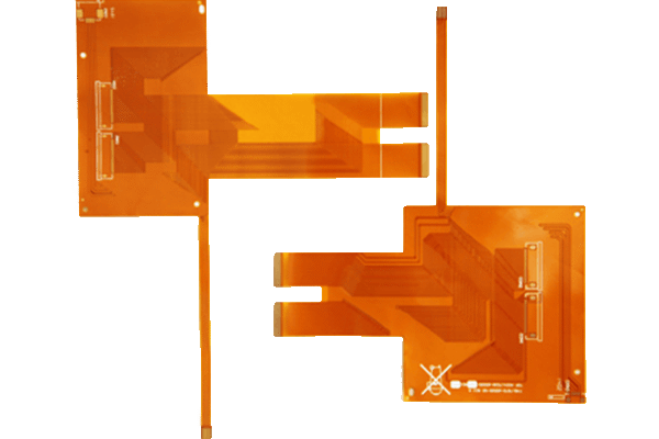
What is High-Density Interconnector PCB (HDI PCB)
HDI, or High-Density Interconnector, refers to a PCB with a higher wiring density per unit area compared to conventional PCBs. HDI PCBs feature finer lines and spaces, smaller vias and capture pads, and higher connection pad density. These attributes make HDI PCBs ideal for reducing the size and weight of devices while enhancing their electrical performance. HDI PCBs are manufactured using microvias, buried vias, and sequential lamination with insulating materials and conductor wiring to achieve higher routing density. They are the best alternative to high-layer-count and expensive standard laminated or sequentially laminated boards.
Electrical Performance Requirements of HDI PCB
To meet the electrical requirements for high-speed signals, HDI PCBs must possess specific AC characteristics, such as impedance control, high-frequency transmission capability, and reduced unnecessary radiation. A multilayer design is necessary to implement stripline and microstrip structures. To address signal transmission quality issues, insulating materials with a low dielectric constant and low attenuation ratio are used. Due to the miniaturization and array configurations of electronic components, PCB density must be improved. With the development of assembly methods like Ball Grid Array (BGA), Chip Scale Package (CSP), and Direct Chip Attachment (DCA), PCBs now feature unprecedented high density. Microvias, with diameters less than 150 micrometers, improve assembly efficiency and space utilization, which is crucial for the miniaturization of electronic products.
Various Names for HDI PCB
PCBs with such structures have been known by many different names. In European and American industries, they were called SBU (Sequence Build-Up Process) due to their sequential production mode. In Japanese industries, they were called MVP (Microvia Process) because the vias in these products are much smaller than before. They were also known as BUM (Build-Up Multilayer Board), as traditional multilayer boards are known as MLB (Multilayer Board). To avoid confusion, the IPC Printed Circuit Association proposed the common name HDI (High Density Interconnection Technology), although this does not fully reflect the characteristics of the circuit board. Thus, the majority in the PCB industry define such products as HDI PCB.

Advantages and Applications of HDI PCB
HDI PCBs offer numerous advantages, such as small size, high speed, and high frequency. They are the main components of personal computers, portable computers, mobile phones, and personal digital assistants. Currently, besides mobile phones, HDI PCBs are widely used in various other consumer products, such as game consoles and MP3 players. Additionally, since 2006, the application of HDI PCBs in notebook computers has been an expected trend in the industry.
Conclusion
HDI PCBs, with their compact, efficient, and high-frequency characteristics, are increasingly becoming the preferred choice for various electronic devices. As technology advances and their application scope broadens, the future of HDI PCBs looks even more promising.