1. Basic principles
1.1 Layout principles
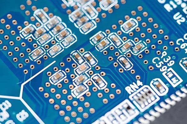
1.1.1 The layout of the components is required to be balanced, dense and orderly, and avoid top-heavy.
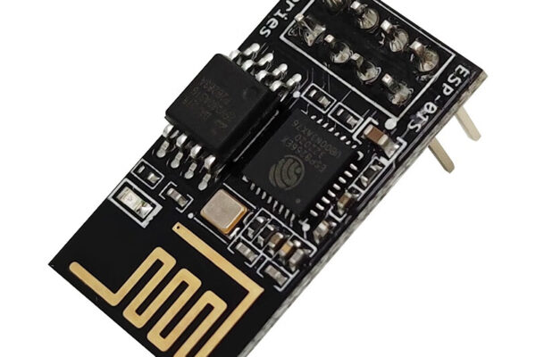
1.1.2 The layout of components should be carried out according to the criticality of components. First, key components such as microprocessor, DSP, FPGA, memory, etc. should be arranged. According to the direction of data lines and address lines, the components should be arranged according to the principle of proximity.
1.1.3 The memory modules are placed side by side as much as possible to shorten the trace length.
1.1.4 Layout as far as possible according to the direction of the signal. Note: The layout of the parts should be considered comprehensively from the aspects of mechanical structure heat dissipation, electromagnetic interference, and convenience of future wiring. First arrange the parts related to the mechanical size, and lock these parts, then arrange the core components of the large parts and circuits, and then the small components of the periphery.
1.2 Wiring principle
1.2.1 Make sure that the width of the wire meets the current-carrying requirements of the wire and leave as much margin as possible. The power and ground wires should be wider, depending on the actual situation. Ground wire>Power wire>Lead wire.
1.2.2 The minimum spacing between the wires is determined by the insulation resistance and breakdown resistance of the wire, and should be as large as possible, generally not less than 12 mils.
1.2.3 When designing the wiring, the traces should be as small as possible to make the lines simple and clear.
1.2.4 The data line address lines of the microprocessor chip should be arranged as parallel as possible.
1.2.5 The input and input side edges should avoid adjacent parallel to avoid reflection interference, and should be isolated if necessary. The two adjacent wires are perpendicular to each other. Parallelism is prone to parasitic coupling.
1.2.6 Improve the stability and anti-interference of PCB by using copper and other processes.
2. Key principle
2.1 Part direction.
2.2 Where the part is placed.
2.3 The width of the wire.
2.4 The layer where the wire is located.