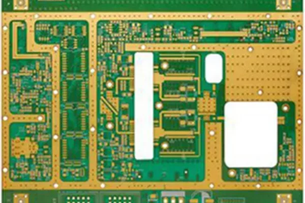
The occurring of solder beading is a complicated process during PCB assembly. Because there are many causes and difficult to control, it often troubles SMT process technicians. Generally, the diameter of the solder beading is between 0.2-0.4mm, and there are some that exceed this range. They are mainly concentrated on the side of the chip (resistor/capacitor) component, and sometimes appear near the IC or connector pins. China PCB manufacturer SYS Technology will introduce today ways to avoid solder beading during PCB SMT process.
Solder beads on PCBA after reflow process
1. Design the stencil opening according to the standard requirements
According to the IPC-7525 stencil design standard, the thickness of the stencil is selected correctly and the opening ratio of the stencil is strictly controlled. Generally, under the condition of ensuring the quality of solder joints, the thickness of the stencil should be selected according to the components with the smallest pin spacing on the PCB. The thinner stencil is preferred, and the thicker steel sheet is to avoid as much as possible.
For chip components of 0603 and above, it is recommended to make anti-solder beading opening, which can effectively solve the problem of solder beading after reflow soldering.
In the SMT surface mount process, the opening method and shape of the stencil may cause some defects in the printing and soldering, thereby causing solder beading. If the opening is improper, it is easy to print the solder paste on the solder resist when printing solder paste, resulting in solder beads during reflow soldering.
In order to solve this problem, without affecting the quality of the solder joints, we can reduce the size of the stencil opening by 10% compared to the actual size of the pad. Experiments have shown that appropriately reducing the size of the stencil opening can effectively reduce the generation of solder beadings. In addition, the shape of the stencil opening can be changed to achieve the desired effect.
2. Improve the cleaning quality of stencil
Improving the cleaning quality of the stencil can improve the printing quality. In the printing process, pay attention to the cleanliness of the surface of the stencil, and wipe the excess residual solder paste on the surface of the stencil in time to prevent the PCB surface from contaminating during the printing process and causing of solder beading during the soldering process. If the stencil is not cleaned, the solder paste remaining at the bottom of the stencil opening will gather near the opening of the stencil, which will contaminate the PCB during printing, and excessive solder paste will form solder beading during reflow soldering.
When chooses the automatic cleaning method of the stencil by printing machine , it is recommended to use the cleaning method of wet wipe, dry wipe and vacuum cleaning modes together, which can improve the effect of stencil cleaning. Specifically, according to the product’s component layout and minimum component pin spacing, the cleaning frequency can be increased appropriately to achieve a good stencil cleaning effect.