Table of Contents
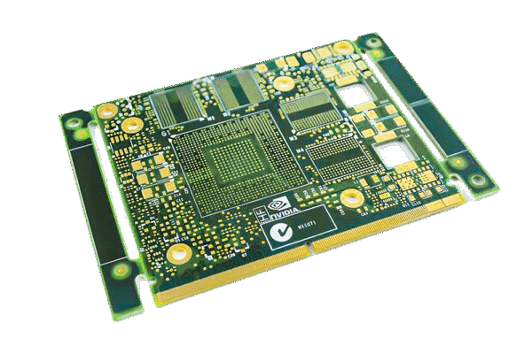
In finished PCBA, Electronic surface mount components are attached directly to the printed circuit board (PCB)
They are also known as SMT components (surface mount technology) or SMD (surface mount devices). Parts are placed according to their position in the signal chain which varies depending on the systems you need to build. For example, if you had a system with an accelerometer, a microcontroller and a USB, the accelerometer would be your input and the USB would be your output. These three parts would need to be placed in that order and within close proximity of one another on the board. You want to keep components related to a certain circuit section close together in order to keep the traces short and reduce noise. Keep in mind that resistance, capacitance and inductance increase with total track length, so it is important to keep tracks as short as possible.
When building any PCB it is easiest to start with the power supply or regulator circuit
This circuit section usually consists of a regulator, a switch, a fuse, and decoupling caps. Usually the switch will be close to the power jack and serve as a hard stop that allows you to cut off all power to the circuit board. You will typically follow the schematic and place a cap on the input, a regulator and a couple more caps on the output to create the regulator circuit that will feed power to the rest of the board. The idea is to find a good secluded location for the power supply components to be placed. Make sure that components which are electrically close on the schematic are physically close on the board.
Star Configuration
Next you want to proceed with a modified star configuration, which means arranging the traces so that each section gets its own dedicated line back to the regulator. This is much easier on a four layer board where there is a second layer of copper underneath that you can punch down to for power, but with a two layer board a little more planning is involved.
Say you had three sections on a circuit, an RF section, a microcontroller section and an op amp section.
Rather than feed each section’s components through a tandem line, the star configuration would involve drawing a trace up to a certain point before drawing lines to each component within the section. That point is your star and allows for the Vcc feed to be split evenly across the different components within a section.
The star configuration prevents the noise that would be introduced if you were to simply chain components together along a single line. If instead we had chained the three sections together, and the first in the chain drew too much power, the other two further down the chain would experience a small voltage drop. As a final note for the star configuration, keep in mind that the initial trace feeding power directly from the Vcc may need to be thicker than the other traces if it is carrying greater than 20 milliamps.


