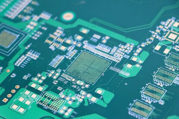
Printed Circuit Boards (PCBs) are essential components in modern electronic devices, and their performance and complexity are largely determined by the number and configuration of layers. Understanding the function and significance of each PCB layer is crucial for efficient design and manufacturing. This article explores the various layers found in a PCB and their roles in ensuring optimal electrical performance and mechanical stability.
Table of Contents
1. Signal Layers
Signal layers are responsible for carrying electrical signals between components. These layers can be classified into:
Top Layer (Component Side): Houses surface-mounted components and primary traces for signal routing.
Bottom Layer (Solder Side): Used for additional routing and sometimes for placing components in double-sided designs.
Internal Signal Layers: Found in multilayer PCBs to facilitate complex routing while minimizing interference.
2. Power and Ground Planes
Dedicated power and ground layers improve electrical performance by providing stable voltage distribution and reducing noise. These layers include:
Power Plane: Distributes power to components efficiently and minimizes voltage drops.
Ground Plane: Acts as a return path for electrical currents, reducing electromagnetic interference (EMI) and improving signal integrity.
3. Dielectric Layers (Substrate)
Dielectric layers separate conductive layers and provide mechanical support. The choice of dielectric material affects factors such as:
Electrical insulation and impedance control.
Thermal stability and heat dissipation.
PCB flexibility (rigid, flexible, or rigid-flex PCBs).
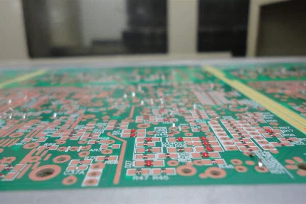
4. Soldermask Layer
The soldermask is a protective coating applied over the copper traces to prevent oxidation, solder bridging, and environmental damage. It is typically green but is available in various colors depending on design preferences.
5. Silkscreen Layer
The silkscreen layer contains printed markings such as component labels, reference designators, logos, and polarity indicators. This layer is essential for PCB assembly, troubleshooting, and maintenance.
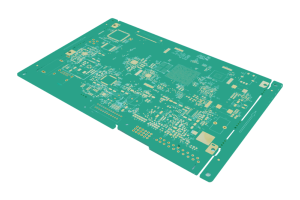
6. Mechanical Layer
Mechanical layers define the physical dimensions of the PCB, including board shape, cutouts, mounting holes, and tooling marks used during manufacturing and assembly.
7. Keep-Out Layer
The keep-out layer specifies restricted areas where no components or traces should be placed. It ensures proper spacing for mechanical clearance, high-voltage isolation, and thermal management.
8. Solder Paste Layer
This layer is used in surface-mount technology (SMT) processes to define where solder paste should be applied for reflow soldering. It ensures accurate placement of solder on component pads.
Conclusion
Understanding PCB layers is fundamental to designing reliable and high-performance circuit boards. Each layer serves a specific function, from signal transmission to mechanical support and protection. As PCB technology advances, designers must carefully consider layer configurations to optimize performance, manufacturability, and cost-effectiveness.