Through-holes are a fundamental feature in the design of multi-layer printed circuit boards (PCBs). These vias, which extend through the entire board to connect different layers, play a crucial role in the electrical performance of a PCB. However, while they are essential for interlayer communication, through-holes can also affect signal transmission, especially in high-speed and high-frequency applications. In this blog post, we will explore how through-holes impact signal integrity, and how engineers can mitigate potential issues to ensure optimal performance in multi-layer PCBs.
Table of Contents
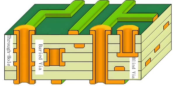
What Are Through-Holes?
Through-holes are conductive paths that connect different layers of a PCB. They are drilled through the entire thickness of the board and plated with copper to create electrical connections between the top, middle, and bottom layers. There are various types of vias, with through-holes being the most common for multi-layer PCBs, where signals need to travel across multiple layers.
The Effect of Through-Holes on Signal Transmission
Inductance and Resistance
One of the primary concerns when using through-holes is their impact on signal transmission, particularly the introduction of inductance and resistance. Through-holes, being relatively large compared to traces, can create an inductive effect that impedes the flow of high-frequency signals. This can lead to signal distortion or degradation, particularly for high-speed digital or RF (radio frequency) signals, where maintaining signal integrity is critical.
The longer the signal path through the via, the greater the resistance, which can result in power loss and signal attenuation. These effects become more pronounced in high-speed circuits, where even small impedance mismatches or delays can significantly affect performance.
Signal Reflection and Impedance Mismatch
Another important consideration is the potential for impedance mismatch caused by the through-hole. In high-frequency circuits, maintaining a consistent impedance along the entire signal path is crucial to prevent reflections. When a signal encounters a through-hole, the via can cause a discontinuity in the impedance, leading to signal reflections. These reflections can result in data errors, decreased signal quality, and overall performance degradation.
Crosstalk Between Layers
In multi-layer PCBs, through-holes can also contribute to crosstalk between adjacent layers. Crosstalk occurs when a signal from one trace induces an unwanted signal in an adjacent trace, which can distort the intended signal. The presence of through-holes can create coupling between different layers, exacerbating crosstalk, especially if the traces are not properly shielded or routed.
PCB Size and Design Complexity
While through-holes are necessary for multi-layer PCBs, their use can increase the complexity of the PCB layout and size. The need for drill holes, plating, and layer transitions can increase manufacturing time and costs. Moreover, through-holes can occupy valuable space that could otherwise be used for routing signal traces, making it harder to achieve optimal layout and routing in high-density designs.
Mitigating the Impact of Through-Holes on Signal Transmission
To minimize the impact of through-holes on signal transmission in multi-layer PCBs, engineers can adopt several strategies during the design process:
Use Blind and Buried Vias
- Blind and buried vias are alternatives to through-holes that can reduce the impact on signal integrity. Blind vias connect outer layers to one or more inner layers but do not pass through the entire board, while buried vias connect only the inner layers and are not visible on the surface. By reducing the need for through-holes, these vias can help lower inductance, resistance, and impedance mismatch, leading to better signal quality.
Minimize Via Lengths
- Reducing the length of through-holes can help lower the inductive and resistive effects. This can be achieved by optimizing the layout to ensure that vias are as short as possible and by strategically placing components to minimize the distance signals must travel through vias.
Impedance Matching
- To minimize signal reflections and impedance mismatch, engineers can implement impedance-controlled via designs. This involves carefully designing the via dimensions (diameter and length) and ensuring that the trace width leading to the via matches the characteristic impedance of the PCB. This technique helps maintain consistent impedance throughout the signal path and reduces the likelihood of signal distortion.
Use of Blind and Buried Vias for High-Speed Signals
- For high-speed or high-frequency signals, using blind and buried vias is particularly effective. Since these vias are more controlled in terms of where they connect and how they interact with traces, they can help reduce crosstalk and signal loss, ensuring that high-performance circuits are not compromised.
Proper Grounding and Shielding
- A solid grounding strategy can reduce the impact of through-holes on signal transmission. Proper grounding and shielding techniques help to isolate signal traces from unwanted interference, ensuring that signals are not distorted by nearby traces or vias. Additionally, ground planes can help minimize the effects of crosstalk and improve overall signal integrity.
Use of Microvias in High-Density Designs
- For high-density designs, microvias are an excellent alternative to traditional through-holes. Microvias are smaller and allow for finer routing, reducing the impact on signal transmission and improving overall performance. They are particularly useful for dense, high-speed, and high-frequency PCB applications.
Conclusion
While through-holes are essential for creating electrical connections in multi-layer PCBs, they can have a significant impact on signal transmission, particularly in high-speed and high-frequency applications. Issues such as increased inductance, resistance, impedance mismatch, and crosstalk can degrade signal integrity and lead to performance problems. However, by carefully considering alternative via types, minimizing via lengths, and implementing impedance matching techniques, engineers can mitigate these effects and ensure optimal signal transmission.
In high-performance designs, particularly those requiring precise signal integrity, it’s crucial to choose the right PCB layout and manufacturing techniques to minimize the impact of through-holes and other via-related issues. Understanding these factors and integrating advanced design strategies can help achieve the best results in multi-layer PCB design.