The Printed Circuit Board (PCB) is the backbone of virtually all modern electronic devices, playing a critical role in connecting and supporting electronic components. Whether it’s a smartphone, a computer, or a medical device, the PCB is essential to the functionality of these systems. However, PCB design and manufacturing involve a complex range of technical terms that can be overwhelming, especially for newcomers. To help demystify the process, this blog post will provide a comprehensive guide to some of the most commonly used PCB technical terms.
1. PCB (Printed Circuit Board)
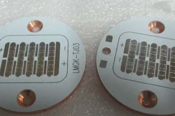
At its core, a Printed Circuit Board (PCB) is a flat board made of insulating material (often fiberglass) with conductive pathways (usually copper) etched or printed onto its surface. These pathways connect various electronic components like resistors, capacitors, and microchips. The PCB serves as both a physical platform for component placement and an electrical interconnection system for the components.
2. Layer Count
PCBs can vary in complexity depending on the number of layers they consist of. Layer count refers to the number of conductive layers in the PCB. The most common types are:
Single-sided PCB: One layer of conductive material (copper) on one side.
Double-sided PCB: Conductive material on both sides of the board.
Multilayer PCB: More than two layers of conductive material, typically used for high-density, high-performance applications like smartphones and computers.
3. Trace
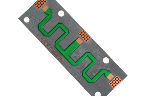
A trace is a conductive path on a PCB that connects various electronic components. It’s usually made from copper and serves as the electrical wiring of the board. The width and thickness of traces are crucial, as they determine the current-carrying capacity of the PCB. The trace pattern is typically designed using PCB design software before the board is manufactured.
4. Via
A via is a hole in the PCB that is plated with copper to connect different layers of the PCB. Vias are used to establish electrical connections between different layers of a multilayer PCB. There are three main types of vias:
Through-hole via: A via that passes through the entire board, from the top layer to the bottom.
Blind via: A via that connects an outer layer to one or more inner layers but doesn’t pass all the way through the PCB.
Buried via: A via that connects only the inner layers and isn’t visible from the outside.
5. Solder Mask
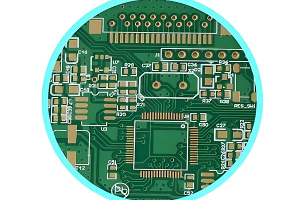
The solder mask is a protective layer applied over the copper traces of a PCB to prevent accidental soldering of components to the wrong areas. This layer is usually green but can come in various colors. It helps protect the board from environmental damage and prevents short circuits caused by unintended solder bridges.
6. Silkscreen
The silkscreen is a layer on the PCB that contains text, logos, and other identifiers, such as component numbers and board labels. This layer is applied on top of the solder mask and aids in the correct placement of components during assembly. It typically uses white ink, but other colors are also possible.
7. Ground Plane
A ground plane is a layer of copper that acts as a common reference point for all the components in the circuit. It provides a low-resistance path for electrical current to flow back to the power source. In addition to reducing noise and improving signal integrity, the ground plane also helps with heat dissipation.
8. Power Plane
Similar to the ground plane, a power plane is a layer of copper dedicated to delivering power to the components on the PCB. It ensures a consistent power supply and reduces the risk of power fluctuations or noise affecting the circuit’s operation.
9. Bill of Materials (BOM)
A Bill of Materials (BOM) is a comprehensive list of all the components required to assemble a PCB. The BOM typically includes part numbers, quantities, manufacturers, and other specifications for the components. It’s an essential document for both the design and manufacturing processes, ensuring that all parts are available and correctly sourced.
10. Pad
A pad is a flat area on the PCB where a component lead is soldered. Pads can be either surface-mounted (SMD pads) or through-hole pads, depending on the type of component being used. Pads provide the necessary electrical connection between the component and the PCB.
11. Impedance Control
Impedance control refers to the management of the electrical resistance encountered by a signal as it travels through the PCB traces. Controlling impedance is crucial for high-speed digital and high-frequency analog signals, as any variation in impedance can result in signal degradation, reflection, or even complete signal loss. Impedance control is typically a design consideration for PCBs used in high-performance applications like telecommunications and networking.
12. PCB Fabrication Process
The PCB fabrication process refers to the series of steps required to manufacture a PCB from a design file. These steps typically include:
Photolithography: A process in which the design is transferred onto the board using light-sensitive chemicals.
Etching: The process of removing unwanted copper to create the trace pattern.
Drilling: The creation of holes for vias and component leads.
Plating: Adding copper to the drilled holes to establish electrical connections between layers.
Solder Mask Application: Applying the protective layer over the copper traces.
Silkscreen Printing: Adding text and component labels to the board.
13. Component Placement
Component placement refers to the process of positioning electronic components on the PCB. The placement must be carefully designed to ensure that the components are properly aligned with the pads, minimizing the risk of errors during assembly. Advanced software tools assist designers in placing components efficiently while also optimizing the layout for performance and manufacturability.
14. Design Rule Check (DRC)
Design Rule Check (DRC) is a verification process used in PCB design software to ensure that the layout meets the manufacturing capabilities and specifications. DRC checks for issues such as incorrect trace width, inadequate spacing between components, and other potential design flaws that could lead to functional or manufacturing problems.
15. Assembly
PCB assembly refers to the process of attaching components to the PCB. This process can be done manually or via automated systems, such as pick-and-place machines. After component placement, the board undergoes soldering (either through wave soldering or reflow soldering), followed by inspection and testing to ensure proper functionality.
Conclusion
This first part of our comprehensive guide to PCB technical terms provides a solid foundation in understanding some of the essential concepts in PCB design and manufacturing. In the next part of this series, we’ll delve deeper into advanced PCB design terms, including signal integrity, high-speed routing, and more. Whether you’re new to PCB design or looking to refresh your knowledge, understanding these basic terms is the first step in mastering the field of PCB engineering. Stay tuned for Part II!