Table of Contents
The Regulatory Shift: CCC Certification Goes Mandatory
As of August 15, 2025, China’s new CCC (China Compulsory Certification) rules for power banks have fully taken effect. Under these regulations:
– Non-certified power banks are illegal to produce, import, or sell within China
– 5012 power bank certificates and 27,167 battery certificates have been issued to date, reflecting intense industry realignment
– Unannounced factory inspections now enforce production consistency, targeting weak points in raw material selection, process control, and final assembly
This regulatory pivot responds to alarming safety failures—including recalls of nearly 500,000 units from brands like Romoss—where flawed circuit protection contributed to thermal runaway risks despite initial certification.
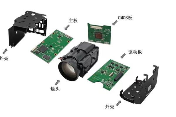
PCB Design: The Critical Enabler of Safety Compliance
While battery cells dominate safety discussions, the PCB is the silent guardian ensuring operational integrity. CCC testing explicitly validates PCB-centric safety functions:
1. Core Protection Circuitry
•Overcharge/Over-Discharge Prevention: Monitors cell voltage, disconnecting load/charge outside safe thresholds (2.5V–4.35V)
•Short-Circuit Response: Must cut output within milliseconds during fault detection
•Thermal Regulation: Uses NTC sensors to throttle current if temperatures exceed 60°C
Failures here directly caused recent recalls when protection delays or false triggers occurred during real-world usage.
2. Precision Power Management
During CCC validation, instruments like the PA300 power analyzer scrutinize:
– Voltage/current stability during load transients
– Actual vs. claimed efficiency (e.g., 85%+ for wireless charging modules)
– Ripple/noise under 2A+ loads, where PCB layout dictates performance
Why Certified Designs Fail: The PCB Consistency Gap
The Romoss incident reveals a harsh truth: certifying a prototype ≠ certifying production units. Key PCB-related failure modes include:
•Component Substitution: Switching to uncertified MOSFETs or current sensors with slower response times
•Solder Joint Defects: Voids/cracks in protection IC connections delaying fault response
•Thermal Design Gaps: Inadequate copper pour causing localized heating during 3A+ fast charging
•Signal Integrity Issues: EMI from poorly routed switching regulators causing false triggering
Designing CCC-Compliant PCBs: Critical Considerations
Table: PCB-Centric CCC Certification Requirements
| Certification Stage | PCB Impact | Mitigation Strategy |
| Electrical Safety (GB 4943.1) | Isolation gaps, creepage distance | ≥3.0mm HV spacing; reinforced insulation slots |
| Battery Safety (GB 31241) | Protection circuit response time | Dual-path sensing; ≤100ns MOSFET drivers |
| EMC Compliance | Switching noise from DC-DC converters | Shielding cans; π-filters; buried power planes |
| Production Audit | BOM consistency across batches | AVL control; traceable component sourcing |
Key PCB Design Rules:
•Protection Circuit Layout: Place voltage/current sensors <5mm from cells to minimize noise-induced errors
•Thermal Management: Use 2 oz copper + thermal vias under MOSFETs to limit ΔT to <15°C at 3A loads
•Testability: Include 0.5mm test pads on all protection signal lines for in-circuit validation
•Material Selection: High-Tg laminates (≥170°C) to survive reflow and environmental stress tests
Case Study: How Robust PCBs Avert Certification Failures
A Tier-1 power bank manufacturer reduced test failures by 70% after implementing:
– HVI (High-Voltage Isolation) Slots: Between AC-DC and battery sections to pass 3kV hipot tests
– Guard Rings: Around voltage sense traces to prevent leakage current errors
– Automated Optical Inspection (AOI): For 100% solder joint validation on protection ICs
Partnering for Compliance: A PCB Manufacturer’s Role
As a PCB specialist, enabling client certification requires:
1.Material Science Expertise
–Recommending high-Tg FR-4 or polyimide blends for thermal endurance
–Selecting low-loss dielectrics for noise-sensitive analog sensing circuits
2.Manufacturing Precision
–Controlling etch tolerances ≤±10% for impedance-critical paths
–Ensuring plating uniformity in microvias for even current distribution
3.Testing & Validation
–IST (Interconnect Stress Test): Simulates thermal cycling to predict field failures
–TDR Testing: Verifies impedance control in protection signal lines
4.Documentation Support
–Providing IPC-6012 Class 2/3 reports for reliability claims
–Generating material certifications for CCC audit trails
The Future: PCBs in Next-Gen Power Safety
With solid-state batteries and GaN fast-charging entering the market, PCB demands will intensify:
– Embedded Current Sensors: Shunt resistors integrated into inner layers for space savings
– AEC-Q200 Qualified Materials: For automotive-grade power banks supporting 48V systems
– 3D Printed Circuits: Enabling conformal layouts within curved battery cells
In China’s CCC-compliant power bank market, the PCB is no longer a passive carrier—it’s the active guardian of safety. By mastering protection circuitry, thermal management, and manufacturing consistency, PCB manufacturers become indispensable partners in navigating certification. Those who prioritize precision and partnership will power the next generation of trustworthy energy storage.
Ready to Design CCC-Certified Power Banks?
→ [Download Our PCB Layout Checklist for GB 31241 Compliance]
→ [Request a Free DFM Review for Protection Circuits]
→ [Explore Our AEC-Q200 Capable Materials Portfolio]