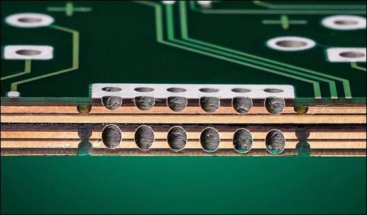
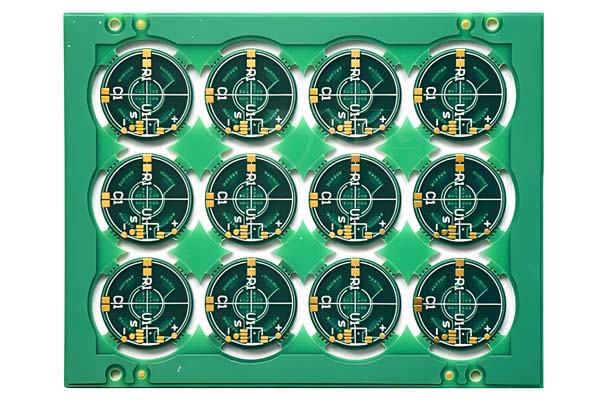
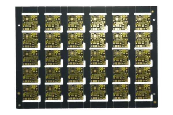
The substrate most commonly used in printed circuit boards is a glass fiber reinforced (fiberglass) epoxy resin with a copper foil bonded on to one or both sides. PCBs made from paper reinforced phenolic resin with a bonded copper foil are less expensive and are often used in household electrical devices. You can make simple PCB by yourself easily, see Shenzhen PCB manufacturer SysPCB’s instruction as below.
The printed circuits are made of copper, which is either plated or etched away on the surface of the substrate to leave the pattern desired. The copper circuits are coated with a layer of tin-lead to prevent oxidation. Contact fingers are plated with tin-lead, then nickel, and finally gold for excellent conductivity.
Table of Contents
Circuit board Design
The design process of the photo etched board can be finished quickly with the use of PCB designing software, available for your computer. Eagle by Cadsoft Online is a PCB design suite containing a layout editor, schematic editor and autorouter, all accessible through a single user interface. It’s available for Windows, Mac and Linux in both a professional version and a freeware light edition.
After designing your board, print the circuit onto transparent paper. Most printers can be programmed specifically for transparent paper but if there is no specific option you should go with the highest quality print options available. With printers containing only black ink, change the intensity and contrast of the printer to the highest levels possible to ensure that you get a clear, clean print using as much black ink as possible.
Preparing the PCB
Print the design onto your transparent paper. Most laser-printer compatible transparencies are made to be printed on a single side only as printing on the wrong side will give you a blurry image. The correct side tends to feel slightly sticky to the touch. Print two transparencies for best results.
After printing the design, trim the transparencies down taking care not to damage the ink when cutting the paper. Take a thin glass panel large enough to hold the design and secure the transparencies to it using transparent tape.
Take the photo PCB that comes prepared with a photo-resist substance and remove the protective covering. Secure the PCB board with the photo-resist layer on the transparency. Looking through the glass you should see the design centered with the transparency held between the glass and the PCB.

Exposing the Design
Place the PCB in your exposure unit, copper side facing the ultraviolet light. Wait the necessary exposure time, based on the manufacturer’s instructions or upon previous experimentation. Exposure transfers your design onto the copper surface, by hardening the photo resist in the shape of the design. While the copper is going through the exposure process you can prepare the developer solution.
The developer solution removes the photo-resist from areas of the PCB not hardened by the UV light. Once exposed, remove from the light unit and from the glass panel. Quickly place the board into your developer. Take a foam brush and brush the photo resist off the board for 1 to 2 minutes. This green resist should come off quickly so take care not to remove the hardened resist. When you’ve removed the unhardened resist, move the board to water in order to neutralize the developer.
Etching the PCB
Make your ferric chloride solution, mixing the ferric chloride with water. Submerge the board into the solution, which will etch your design by removing the unneeded copper from the board, leaving copper only on the lines of your design. Once the design is etched into the surface of the board, remove from the solution and wash the PCB with running water.
Clean the remaining photo-resist from the copper lines on your PCB using the acetone. As you clean away the photo-resist, the copper will appear brighter. Wash again with running water, and then drill the holes where needed according to the design using either a hand drill or a drill press.
Drill
Then you put PCB under in a CNC machine or small tools for drilling you got, and the holes are drilled according to the pattern determined when the boards were laid out. The holes are deburred to remove any excess material clinging to the edges of the holes. This method gives the DIY electrician crisp clean lines on their PCB boards in a short amount of time at little expense and with few necessary materials. Get start, make your own PCB today.


