PCB Manufacturing Process Optimization Guide: Seven Key Control Points from Design to Delivery
Against the backdrop of rapid development in 5G communication, artificial intelligence, and automotive electronics, the global PCB industry is facing three major challenges: high frequency, high density, and high reliability. According to industry data, the high-frequency PCB market size is expected to exceed $14.2 billion by 2025, with rework costs caused by manufacturing defects reaching over $85 per board. As a technical team with 16 years of experience in the PCB industry, we will analyze the core control elements of high-performance PCB production from seven dimensions.
Table of Contents
1、 Design side manufacturability planning (DFM): preventive optimization
Layout and wiring rules
-Space constraint: The spacing between 0402 components should be ≥ 0.2mm, and mechanical through holes should be avoided in the BGA area. Laser blind holes (aperture ≤ 0.1mm) should be used instead to reduce signal reflection.
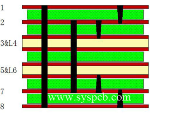
-Stacked architecture: It is recommended to use the “Top GND Signal Power Signal Bottom” structure for 6-layer boards, with impedance control accuracy of ± 7% (PCIe 5.0 requires ± 5%).

Process limit adaptation
-Line width/spacing ≥ 3/3mil (laser process) or 6/6mil (conventional process), steel mesh hole ratio differentiated design according to component type (such as 0402 component 1:1, QFN pad expansion of 20%).
2、 Raw Materials and Supply Chain Management: Balancing Performance and Cost
Substrate selection matrix
| Application scenarios | Recommended materials | Key parameters | Cost coefficient |
| 5G base station (28GHz) | Rogers RT/duroid 6035 | Df ≤ 0.0019, CTE=17ppm/℃ | 4-5 × FR-4 |
| Automotive Electronics | Isola IS680 | Tg=220 ℃, temperature resistance -40~150 ℃ | 2-3 × FR-4 |
| Consumer Electronics | Shengyi Technology S7136H | Halogen free, Df=0.0035 | 1.2 × FR-4 |
Supply Chain Resilience Strategy
-Implement dual source certification for key materials such as ABF film and high-frequency copper-clad laminates, and establish an inventory warning system (safety stock ≥ 15 days).
3、 Production process and equipment accuracy: the core guarantee of yield
Key control points for hole machining
-Drilling accuracy: Laser drilling positioning error ≤ ± 10 μ m (HDI board requirement), mechanical drilling uses nano coated drill bits to reduce CCL wear.
-Electroplating uniformity: The copper thickness tolerance is controlled within ± 3 μ m through pulse electroplating technology to avoid hole wall fracture.
Optimization of etching process
-Real time monitoring of the composition of the medicine (Cu ² ⁺ concentration ± 5g/L), using vacuum etching lines to reduce side corrosion (burrs ≤ 1.5 μ m).
4、 Quality system and standard compliance: 6 Sigma drives zero defects
Process monitoring technology
-SPC system: Real time tracking of line width deviation (± 5%) and interlayer alignment accuracy (± 25 μ m).
-Failure prevention: FMEA analysis identifies risk points such as pad delamination and CAF failure in advance, and implements corrective measures.
reliability verification
-100% flying needle test+temperature and humidity cycling test (-55 ℃~125 ℃, 500 cycles) meets IPC-6012E Class 3 standard.
5、 Cost and Efficiency Optimization: Lean Manufacturing Practice
Cost reduction and efficiency improvement leverage
-Design simplification: Replace through holes with blind buried holes to reduce the lamination process by 30%; Optimizing the size of the panel improves material utilization to 92%.
-Automation upgrade: AOI detection speed has been increased to 5 pieces/minute, and the misjudgment rate has decreased by 70%; The LDI exposure accuracy reaches 20 μ m.
Supply Chain Collaboration
-Implement JIT material distribution and increase inventory turnover to 12 times per year.
6、 Environmental Protection and Sustainable Production: Compliance Competitiveness
Breakthrough in Green Technology
-Lead free soldering: Using SAC305+Bi alloy (melting point 217 ℃), energy consumption is reduced by 15%.
-Waste recycling: The copper recovery rate of etching waste liquid is ≥ 99%, and the wastewater reuse rate is increased to 80%.
Certification system
-Advance layout of RoHS 3.0 and ISO 14064 certification to meet Apple/Samsung’s green supply chain requirements.
7、 Technology and Demand Adaptation: Building Future Competitiveness
Frontier technology layout
-Material innovation: Nano alumina filled resin (Df reduced by 40%), fluorinated graphene substrate (Df ≤ 0.001).
-Technological Revolution: mSAP technology achieves 10/10 μ m line width and embedded component PCB (volume reduction of 30%).
Market driven research and development
-6G communication: Developing Df ≤ 0.001 board to cope with 120GHz frequency band
-AI server: Optimize ± 5% impedance control of 56Gbps PAM4 signal.
>Case study: After a certain automotive electronics customer adopted high-frequency plates with CTE ≤ 25ppm/℃, the thermal stress failure rate decreased by 90% and the Tier 1 order share increased by 35%.
Conclusion: Building Resilient Manufacturing Systems
PCB manufacturing is a deep coupling of materials science, process engineering, and intelligent management. Faced with the technological wave of AI and 6G, enterprises need to build a full chain control system of “design material process testing”:
-Short term strategy: Import DFM automated inspection tool to shorten the design iteration cycle by 50%
-Long term layout: Building zero carbon factories (photovoltaic power supply+wastewater recycling), reducing carbon emission intensity by 40%
→ [Obtain the High Reliability PCB Manufacturing Checklist], covering IPC-A-600H standards, high-speed material selection guidelines, and the 6 Sigma implementation framework.
Get your exclusive quote immediately: fill out the form or send an email directly.As a professional PCB manufacturer for hobbyist , we will provide you with a quote service within 24 hours. Enjoy free DFM optimization and a 10% discount on SMT patches for your first order!