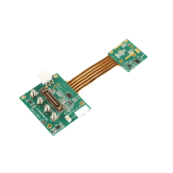
In the field of flexible circuit boards (FPCs), the cost of failure caused by design defects can account for over 30% of the total development cost. As the “dynamic nerve” of electronic devices, FPC needs to maintain signal integrity under extreme conditions such as bending, high temperature, and vibration, and the IPC-2223 standard is the gold standard for achieving this goal. This article will combine the core clauses of the standard with industry practices to break down the core technical points of FPC design for you.
—
Table of Contents
1、 Material selection: Genetic engineering of flexible circuits
Scientific matching of substrate and adhesive
-Polyimide (PI) film: As the preferred substrate for IPC-2223, its thermal stability (temperature resistance>260 ℃) and mechanical toughness (modulus 4000MPa) far exceed polyester (PET), making it particularly suitable for automotive electronics and medical equipment that require reflow soldering.
-Adhesive type: For dynamic bending scenarios (such as folding screen hinge areas), priority should be given to non adhesive lamination processes to avoid the risk of interlayer separation caused by low Tg (glass transition temperature) of epoxy resin adhesives; A lower cost acrylic adhesive can be used for static scenes.
The critical rule for selecting copper foil
-Repeated bending application: It is necessary to use rolled toughened copper (RA copper), which has a 50% increase in Z-axis ductility compared to electrolytic copper (ED copper), and a bending life of more than 100000 times (such as mobile phone flip hinge FPC).
-High current scenario: 2oz ED copper foil achieves high current carrying capacity through etching differential technology, but it should be avoided for use in the bending area.
—
2、 Core Design Rule: From Theory to Production Line Adaptation
1. Design specifications for text and signage
-Position and size: The characters must be placed in the outer area of the board, with a fixed height of 0.8mm and a line width of ≥ 0.12mm, to ensure clear screen printing and not affect welding.
-Bottom level image processing: Draw in the forward direction during design, and mirror processed by the manufacturer during production to avoid reverse errors.
2. Reliability password for via design
| Design Scenario | IPC-2223 Requirements | Failure Avoidance Plan |
| Half hole at the edge of the board | Hole diameter ≥ 0.3mm | Elliptical solder pad+0.3mm copper ring reserved inside the board |
| Bending area through hole | No opening windows | Full hole covered with solder mask |
| Dense via holes | Hole spacing ≥ 0.5mm | Misalignment layout (offset 0.3~0.5mm) |
Data integration from IPC-2223B
>Case warning: When the through-hole spacing is less than 0.45mm, the wicking effect can cause chemical solution penetration, leading to CAF (conductive anode wire) short circuit and a failure rate soaring by 80% in humid environments.
3. Micro level control of solder pads and circuits
-Pad size: 0201 component pad aspect ratio of 1.3:1 (e.g. 0.6 × 0.3mm component with 0.78 × 0.39mm pad), 0.4mm spacing IC pad width=spacing × 0.5.
-Copper laying trap: Avoid large areas of solid copper laying! Using grid copper (line width/spacing=0.2mm/0.2mm) and adding breathable windows to prevent compression bubbles and welding delamination.
—
3、 Special structural design: The survival rules of bending zone and golden finger
▶ The ‘Three No’s Principle’ of Dynamic Bending Zone
1. Non windowed solder pad: The solder mask must completely cover the solder pad to avoid bending stress concentration that may cause fracture.
2. Seam without covering film: The seam should deviate from the bending axis by ≥ 2mm to prevent delamination after repeated bending.
3. Wireless right angle: The angle between the routing direction and the bending line is ≥ 90 °, and a circular arc transition is used to reduce stress.

▶ Reinforcement design for golden fingers
-Welding type gold finger: The front and back of the solder pad are misaligned by 0.3mm, and half holes are added to enhance mechanical anchoring.
-Plug in type gold finger:
·Mathematical formulas
PI reinforcement thickness=total thickness – (plate thickness – cover film thickness – copper thickness)
Example: When the total thickness is 0.3mm, the plate thickness is 0.11mm, and there is no copper backing plate, 0.25mm PI reinforcement is required (automatically calculated by Jialichuang tool).
—
4、 Process collaboration: a key stepping stone from design drawings to mass production
1. Precise matching of reinforcing plates
-Micro pitch components: Prior to SMT, a PI reinforcement plate resistant to 260 ℃ is added to the back of the component, with a size 1.0mm larger than the solder pad extension, and the anti cracking tin strength is increased by three times.

-Positioning system: Each panel is equipped with 4 Φ 2.0mm positioning holes, with a diagonal distribution error of less than 0.05mm.
2. Selection of solder mask and covering film processes
-Dynamic area: Laser cutting polyimide cover film is used, with a window opening accuracy of ± 0.05mm (better than ± 0.1mm for ink printing).
-Hard board joint: coated with epoxy resin beads (width ≥ 0.5mm) to disperse stress and prevent tearing.
—
5、 Design Verification: Using Tools and Data to Close Loop Risks
Four essential calculation tools (free to use on Jialichuang official website):
1. Current line width calculator: Input current value, copper thickness, temperature rise threshold, and output the minimum safe line width (such as 1.2mm line width required for 1oz copper 10A current).
2. Via current calculator: Calculate the current carrying capacity of a single hole based on the aperture and copper thickness (e.g. maximum current carrying capacity of 1.2A for a Φ 0.3mm hole with 1oz copper thickness).
3. Coil resistance calculator: Derive line width by reversing line length to optimize high-frequency impedance.
4. PI reinforcement thickness calculator: automatically solves the problem of thickness matching.
DFM checklist:
-Gerber file: must include SMT pad layer, MARK point layer, and PCB data layer.
-CAF testing: Submit a report of -55 ℃~150 ℃ cycling>500 times, and special testing is required for plates with hole spacing<0.5mm.
—
Conclusion: Anchored by standards, heading towards a highly reliable and flexible future
IPC-2223 is not only a design specification, but also a reliability philosophy that integrates materials science, mechanical mechanics, and electrochemistry. Behind these “hidden champions” – folding phones that have undergone 100000 bends and new energy vehicle battery management systems that have stable sampling during vibration – is the reverence for every micrometer level rule.
>Erich M ü ller, an expert from the German Industrial Standards Committee, once asserted that:
>The greatness of flexible circuits lies in their ability to carry the most rigid mission with the most humble bending
The technical parameters of this article are based on IPC-2223B and supported by the PCB Technology Alliance.