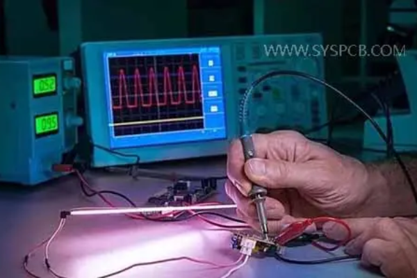
In the world of PCB (Printed Circuit Board) manufacturing and testing, accurate and reliable probing is essential for ensuring the quality and functionality of electronic devices. Probes are used for a variety of tasks, including circuit testing, debugging, quality control, and failure analysis. Depending on the application, the type of probe used can vary significantly. In this blog, we will explore seven common types of PCB probes, each designed to meet specific testing needs in the PCB assembly process.
Table of Contents
1. In-Circuit Test (ICT) Probes
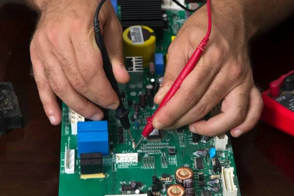
In-Circuit Test (ICT) probes are one of the most common types of probes used in PCB testing. They are part of an ICT machine that is designed to test each component on the PCB while it is still in the circuit. ICT probes make direct contact with test points on the PCB, allowing for the measurement of voltage, current, resistance, and other electrical characteristics. These probes are used to detect faults such as open circuits, shorts, incorrect values, and other issues that could affect the board’s functionality.
Key Features:
Used for testing components in-circuit
Can detect faults in individual components and solder joints
Provides detailed electrical measurements to ensure the board’s integrity
2. Flying Probe Test (FPT) Probes
Flying Probe Testing (FPT) is a non-contact, automated testing method used to check the electrical functionality of a PCB. Flying probe machines use a set of probes that move over the PCB to perform tests, as opposed to the fixed probes used in ICT. These probes are often used for low-volume production or prototype testing where creating a fixture for ICT is not cost-effective. Flying probes can test a range of electrical parameters such as resistance, capacitance, and inductance, and are capable of detecting shorts, opens, and other defects.

Key Features:
Ideal for low-volume and prototype testing
Does not require custom test fixtures
Flexible testing for a wide range of electrical parameters
3. Bed of Nails Probes
Bed of Nails probes, often used in ICT systems, consist of a large array of spring-loaded pins arranged on a fixture that makes contact with test points on the PCB. This type of probing system allows for high-speed, simultaneous testing of multiple points on the PCB. Bed of Nails probes are particularly effective for high-volume production environments where speed and efficiency are crucial. These probes are custom-designed to match the specific layout of the PCB, ensuring accurate contact with the designated test pads or vias.
Key Features:
Provides high-speed testing for mass production
Custom-designed for specific PCBs
Effective for testing a large number of points simultaneously
4. Needle Probes
Needle probes are often used for both manual and automated testing in PCB inspection. These probes have a fine, needle-like tip that allows for precise contact with individual test points on the PCB. Needle probes are commonly used in applications where fine-pitch components and small vias need to be tested. They are often used in conjunction with microscopes or other inspection equipment to ensure that contact is made with the correct pads and vias.
Key Features:
Ideal for fine-pitch components and small test points
Provides precise and accurate testing
Used in both manual and automated test setups
5. Microscopic Probes

Microscopic probes are used in failure analysis, inspection, and high-precision testing. These probes are equipped with very fine tips and are often used for inspecting smaller, more complex components such as microvias, fine-pitch connectors, and small components that are difficult to test using other methods. These probes are commonly used in conjunction with electron microscopes (SEM) or optical microscopes to provide high-resolution imaging and precise probing.
Key Features:
Designed for high-precision testing and failure analysis
Used for inspecting microvias and fine-pitch components
Often combined with advanced microscope systems for enhanced imaging
6. Thermal Probes
Thermal probes are used to detect temperature variations on the PCB during operation or testing. These probes are critical for identifying overheating issues that could cause components to fail or degrade over time. Thermal probes typically include infrared sensors or thermocouples that can measure surface temperature with high accuracy. This type of probing is essential for thermal analysis during the reflow soldering process or for identifying potential hot spots on PCBs during operation.
Key Features:
Measures temperature variations on the PCB surface
Critical for identifying overheating issues
Useful during reflow soldering or operation to detect hot spots
7. Laser Probes
Laser probes are advanced tools used for non-contact measurements and inspection of PCBs. These probes use laser beams to detect the surface profile, height, and alignment of components and traces on the PCB. Laser probes are highly accurate and are often used for inspecting the integrity of the PCB during the assembly process or for post-production testing. They can be used to verify solder joints, component placement, and other critical parameters with precision and without physically touching the PCB.
Key Features:
Non-contact measurement and inspection
High-accuracy surface profiling and alignment checking
Ideal for post-production and quality assurance
Conclusion
The choice of PCB probe depends largely on the specific testing needs and requirements of the manufacturing process. Each type of probe has its strengths and is designed to meet particular challenges in PCB testing, whether it’s for detecting electrical faults, ensuring precise component placement, or identifying thermal issues. By understanding the different types of probes available and their applications, manufacturers can optimize their testing processes and improve the overall quality and reliability of their PCBs.
Whether it’s for high-volume production, low-volume prototypes, or advanced failure analysis, selecting the right PCB probe is essential for ensuring that the final product meets both functional and quality standards. In today’s competitive electronics market, precision and efficiency in testing are key to delivering reliable, high-performance devices.
Get your exclusive quote immediately: fill out the form or send an email directly.As a professional PCB manufacturer for hobbyist , we will provide you with a quote service within 24 hours. Enjoy free DFM optimization and a 10% discount on SMT patches for your first order!