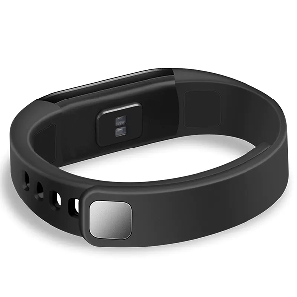
As a portable wearable device, the PCB design of smart bracelets needs to balance functionality, reliability, and miniaturization requirements. The following outlines design considerations from multiple key dimensions:
Table of Contents
Ⅰ. Overall layout planning
1. Size and form adaptation
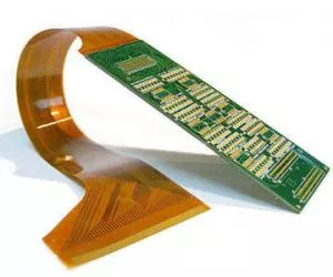
-Bracelets are usually in the shape of long strips or rings, and the PCB should be designed as curved or flexible (FPC) according to the curvature of the strap to avoid hard bending that may cause solder joints to crack.
-The thickness should be controlled within 0.8-1.2mm, and assembly space should be reserved for component heights (such as batteries and sensors) to ensure that the overall thickness of the machine is ≤ 15mm.
2. Module partitioning principle
| Functional modules | Layout key points |
| Main control chip area | Near the battery power supply end, sufficient ground plane is reserved around to reduce power noise interference. |
| Sensor area | The accelerometer and heart rate sensor should be close to the inside of the watch strap, away from metal components (such as charging contacts), to avoid magnetic field interference. |
| The communication module | Bluetooth/Wi Fi antenna should be placed at the edge of the PCB, away from shielding covers and large-sized metal parts, to ensure signal radiation efficiency. |
| Battery and Charging | Lithium batteries should be laid flat in the center of the PCB as much as possible, and charging contacts (such as Pogo pins) should be aligned with the housing openings to avoid misalignment. |
3. Heat dissipation design
-A copper foil heat dissipation area is laid below the main control chip, connected to the inner ground plane through vias to reduce temperature rise during long-term use (target ≤ 45 ℃).
Ⅱ. Key points of electrical design
1. Power management optimization
-Low power LDO (Low Dropout Linear Regulator) is used to power the sensor, with ripple controlled within 50mV to avoid affecting data acquisition accuracy.
-The battery charging and discharging circuit needs to integrate an overcharge/overdischarge protection chip, with a charging current of ≤ 100mA (suitable for 50-150mAh batteries) to prevent overheating.
2. Signal integrity design
-The length of the I2C/SPI signal line for the sensor should be ≤ 10mm, and the differential wiring (such as heart rate signals) should be kept equidistant and of equal length. The impedance should be controlled at 100 ± 5 Ω.
-Crystal oscillators (such as 32.768kHz clocks) need to be isolated with a metal shielding cover, and high-speed signal lines are prohibited from passing underneath to avoid frequency jitter.
3. Anti interference measures
-Digital ground and analog ground are connected through a 0 Ω resistor or magnetic bead single point connection to prevent ground loop interference with sensor signals (such as heart rate fluctuation misjudgment).
-The outer layer of the PCB is laid with a complete grounding plane, and a grounding via array (spacing ≤ 1mm) is set around key components (such as MCU).
Ⅲ. Process and Manufacturing Requirements
1. Material selection
-FR-4 (dielectric constant ε r=4.4) or Rogers RO3003 (ε r=3.0) are recommended for high-frequency boards to reduce signal loss, especially in the Bluetooth antenna area.
-Flexible PCB (FPC) should use polyimide substrate with a bending radius of ≥ 3mm to avoid repeated bending and circuit breakage.
2. Solder pad and routing design
-0402/0201 packaging components account for ≥ 80%, pad spacing ≤ 0.3mm, and wire width ≥ 5mil (0.127mm) to ensure small-scale assembly.
-The battery pads need to be treated with tin coating, with an area of ≥ 2mm × 2mm, to enhance the welding firmness (to avoid detachment during movement).
3. Testing and assembly
-Reserve BGA solder ball test points (diameter ≥ 0.3mm) for convenient functional debugging; The FPC connection area needs to be designed with foolproof positioning holes to avoid assembly misalignment.
-The ENIG process is preferred for surface treatment, which has better antioxidant capacity than OSP and is suitable for long-term wearing scenarios.
Ⅳ.Special function design
1. Heart rate monitoring module
-Optical heart rate sensors (such as PPG) need to be close to the PCB surface, with transparent holes aligned with the housing lens, and surrounded by shading ink to isolate environmental light interference.
-The distance between the light source (LED) and the photodiode is controlled at 1.5-2mm to ensure the stability of the light signal reflection path.
2. Waterproof structure coordination
-The edges of the PCB need to be coated with waterproof material (such as Parylene), and the through holes at the button/charging interface should be sealed with resin plugs and gold-plated to prevent water vapor from seeping in.
-The sealing gasket groove should be reserved with a positioning protrusion on the PCB to ensure that it meets the IP68 waterproof rating after assembly with the housing.
Ⅴ.EMC and Compliance
-The radiation stray of Bluetooth antenna must comply with FCC Part 15.247 standard, with a radiation intensity of ≤ 40dB μ V/m in the 30-1000MHz frequency band.
-The electrostatic discharge protection (ESD) of the whole machine needs to pass the ± 8kV contact discharge test, and TVS diode protection needs to be added to the key signal layer of the PCB.
Ⅵ.Cost and Mass Production Optimization
-The panel design adopts V-Cut or stamp hole connection to improve the utilization rate of FPC/PCB (the number of single panel panels is ≥ 10) and reduce production costs.
-Priority should be given to selecting small package and low-power models (such as STM32L series MCUs) for component selection, to avoid the impact of non-standard interfaces on surface mount efficiency.
By controlling the above design points, it can ensure that the smart bracelet PCB meets the strict requirements of wearable devices in terms of miniaturization, low power consumption, and reliability, while reserving expansion space for subsequent functional iterations such as blood oxygen monitoring and GPS integration.
Get your exclusive quote immediately: fill out the form or send an email directly.As a professional PCB manufacturer for hobbyist , we will provide you with a quote service within 24 hours. Enjoy free DFM optimization and a 10% discount on SMT patches for your first order!