With the continuous growth of new energy demand and the transformation of the energy structure, the market size of energy storage technology continues to expand. As an important part of battery modules in energy storage systems, energy storage PCBs play a key role in the safety and performance of the entire system. Today we will talk about the layout considerations and manufacturing difficulties of energy storage PCBs.
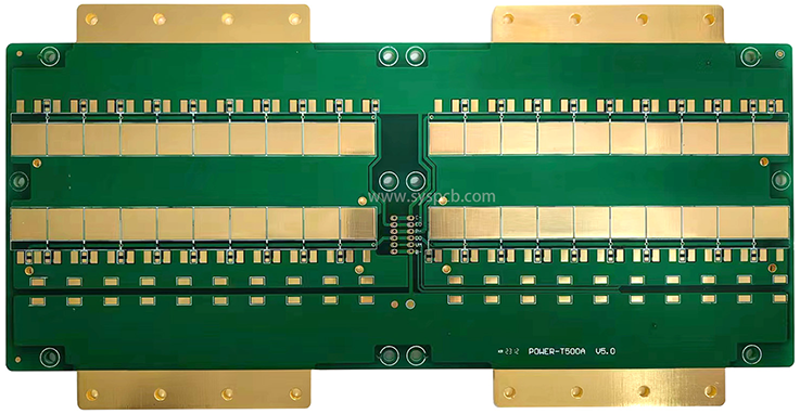
Table of Contents
1. What are the characteristics of energy storage PCB boards?
1. It is difficult to find BGA chips and some fine-pitch devices on energy storage PCB boards; they are mainly focused on charging and discharging.
2. Energy storage boards generally have thicker copper, mostly 2 oz or more; they are mainly high-current, accompanied by high voltage (up to kilovolts).
3. Also because of high-current operation, the board is more prone to heat generation. Therefore, energy storage PCB boards are usually designed with heat dissipation measures, such as adding thermal vias or adding some packaged heat sinks.
2. What should be noted in the design and manufacturing of energy storage PCBs?
First, due to the presence of high current, the power ground will be disturbed when high current flows through it; second, during the variation of high current, EMC interference radiation is easily generated.
Therefore, when designing and manufacturing energy storage PCBs, we should pay attention to the following points:
1. Choose high-performance materials suitable for high-current applications as much as possible, such as FR-4, metal substrates, and composite materials. These materials have lower resistance, higher thermal conductivity, and good mechanical strength, and can withstand heat and current concentration effects under high current.
2. Balance current distribution. Reasonable current distribution can reduce the resistance of the current path and the generation of hot spots. For example, adding current balancers, balancing resistors, or current balancing layers can improve the reliability and stability of the circuit board.
3. When routing PCB traces, try not to cross high-current paths with digital signals to avoid mutual interference.
4. High-current paths should be treated with solid copper fill as much as possible. First, the current-carrying capacity is relatively large; second, it provides better heat dissipation; third, it avoids high trace impedance and large voltage drop on the traces.
5. Heat generated by high current can damage components and products, so the power path deserves even more attention. Generally, large-area copper pour, vias, and opening the external solder mask to expose copper are used to accelerate heat dissipation.
6. During layout, consider the EMC radiation problem of high current. Methods such as increasing trace width, increasing aperture size, and increasing spacing can be adopted. High-current paths should be as short as possible, and when planning the path, keep it away from devices susceptible to interference (signal interference and thermal effects).
3. What are the difficulties in manufacturing energy storage PCB boards?
Because of the influence of high current, thick copper boards are generally required, and thick copper boards will encounter processing difficulties such as the following during production and manufacturing.
1. Etching difficulties
Because the copper thickness increases, chemical exchange becomes more difficult. To minimize excessive side etching caused by chemical exchange, multiple rapid etchings are required. As side etching increases, it is also necessary to compensate for side etching by increasing the etching compensation coefficient.
2. Lamination difficulties
As copper thickness increases, the line gaps become deeper, and the amount of resin filling required increases accordingly. Since resin is needed to fill line gaps and other areas to the maximum extent, prepreg with high resin content and good resin fluidity is the first choice for thick copper boards. However, an increased amount of prepreg also increases the risk of slippage. A common method is to add rivets to strengthen the fixation between core boards.
3. Drilling difficulties
Thick copper boards usually have a board thickness of 2.0 mm or more. When drilling, X-RAY energy gradually attenuates as copper thickness increases, and its penetrating ability reaches its upper limit. There may also be the problem of pad cracking during PCB drilling. Traditional improvement methods include increasing the pad size, increasing the peel strength of the material, and reducing the drill bit landing speed.
China PCB manufacturer SysPCB has been deeply engaged in the PCB industry for more than 10 years. We have rich production experience in energy storage PCB boards. SysPCB has also always been working to improve process capability and can meet various customer needs for products. SysPCB has always been committed to providing high-reliability multilayer board for customers, focusing on PCB and PCBA manufacturing, and providing customers with high-reliability and short lead-time board manufacturing experience.