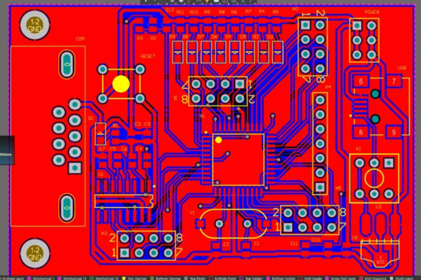
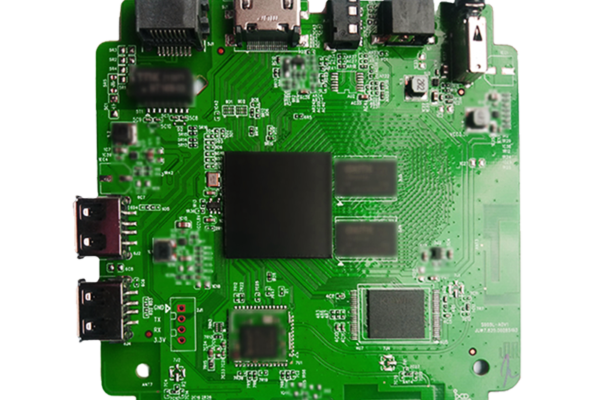
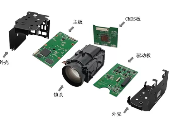
From PCB design to finished electronic products—small tools, smartphones, home appliances or electrical appliances, and all electronic product devices you can think of and see—PCB circuit board prototypes are very important. They allow a given design to be tested to determine whether it works. This makes it possible to debug and correct any errors. This is also very useful before mass production. Without a PCB prototype, mass production of electronic circuit boards and related products still carries risks.
In complex circuit boards, minor errors can be very expensive and time-consuming and difficult to correct. A flawed design can make soldering electronic components very difficult. It also becomes more difficult to pinpoint the error on the board. Therefore, it is wise to design and prototype a PCB circuit board before actual production to avoid any future risks.
Table of Contents
Now let us introduce what a PCB circuit board (Printed Circuit Board) is.
Most electronic devices and products have PCB circuit boards. A printed circuit board (PCB / PWB) is a board made of non-insulating and highly heat-resistant insulating material (such as fiberglass). These boards are also called substrates. A PCB substrate can have only a single layer (single-sided circuit board) or more than one layer (multilayer circuit board). Conductive metals such as copper are used to create conductive paths or traces to facilitate current flow. Once PCB soldering is completed, it is called a “printed circuit board.” After electronic components are soldered, the same PCB is called a printed circuit board assembly (PCBA).
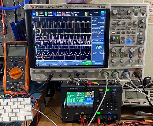
PCB Circuit Board Prototyping
When designing a new circuit, it is very important to draw the circuit board schematic beforehand. The circuit board schematic will help debug and fix any errors that occur during the process. If the circuit on the board is simple, a very simple and easy-to-understand prototype board can be used. In the case of complex and customized circuit boards, making a prototype PCB board is necessary.
Design Software for PCB Circuit Board Layout
To start making a PCB circuit board prototype, circuit board fabrication data such as Gerber files are required. PCB layout software can be used for this purpose. Circuit board layout software draws the board layout with all traces and indicates where electronic components will be soldered on the board. The PCB layout looks like a diagram. PCB layout software allows the layout to be edited until the desired layout is achieved.
How to Make a PCB Circuit Board?
Manufacturing a PCB circuit board involves several complex processes.
1. Film exposure/imaging:
In this process, a mask or photomask is combined with chemical etching to subtract copper areas from the PCB substrate. The photomask is created using a photoplotter based on a design made with a CAD PCB software program. Photomasks are also created using laser printers.
2. Lamination:
Multilayer PCB circuit boards consist of multiple thin etched boards or trace layers and are bonded together through a lamination process.
3. Drilling:
Each layer of a PCB circuit board needs the ability to connect to another layer; this is achieved by drilling small holes called “vias.” Drilling is mainly done using automated computer-driven drilling machines.
4. Pad tinning/surface finish:
The soldering points of electronic components on the PCB pads are tinned or chemically gold-plated so that electronic components can be soldered. Bare copper is not easy to solder. It requires a surface plated with a material that facilitates soldering. Earlier lead-based tin was used to plate the surface, but with RoHS (Restriction of Hazardous Substances) compliance, newer lead-free materials such as nickel and gold are now used for plating.
5. Testing the PCB circuit board:
Before electronic components are soldered onto the PCB circuit board, it needs to be tested. This test can use a test fixture tester or flying probe testing. A flying probe tester is another computer-operated circuit board testing device.
Whether for PCB circuit board prototyping or mass manufacturing, the manufacturing process and procedural steps are similar; the only difference is that the cost of manufacturing PCB prototypes and the upfront tooling costs amortized in mass manufacturing are different.
Conclusion:
When manufacturing PCB prototypes, it is very important to follow the rules from film imaging to testing. Any minor error can make the PCB circuit board useless. In the case of mass production, PCB prototyping is necessary. Before prototyping, there must be a perfect PCB design for manufacturability. Due to the lack of simple and practical design-for-manufacturability analysis tools, most engineers directly ignore the DFM analysis process during design. This causes a large number of design risks to flow into production, ultimately leading to a series of problems such as scrapped PCB boards, delayed development cycles, and missed product launch opportunities.