In PCB manufacturing, due to differences in technical requirements and manufacturing capabilities, there are many special processes with high technical thresholds, difficult operation, high cost, and long lead times.
1. Impedance Control
When digital signals are transmitted on the board, the characteristic impedance of the PCB must match the electronic impedance of the components at both ends. Once they do not match, the transmitted signal energy will experience reflection, scattering, attenuation, or delay. In this case, impedance control must be performed to match the characteristic impedance of the PCB with the components.
2. HDI Blind and Buried Vias
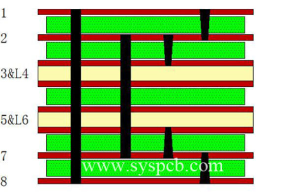
Blind vias are visible only on one of the top or bottom layers; buried vias are vias in the inner layers, with both the top and bottom surfaces of the hole located in the internal layers of the board. The application of blind and buried vias greatly reduces the size and weight of HDI (High-Density Interconnect) PCBs, reduces the number of layers, improves electromagnetic compatibility, reduces costs, and also makes design work simpler and faster.
3. Thick Copper Boards
A layer of copper foil is bonded to the outer layer of FR-4. When the finished copper thickness is ≥ 2 oz, it is defined as a thick copper board. Thick copper boards have excellent elongation properties, resistance to high and low temperatures, and corrosion resistance, giving electronic products a longer service life and greatly helping to miniaturize product volume.
4. Multilayer Special Stack-Up Structures
The stack-up structure is an important factor affecting the EMC performance of PCB boards and is also an important means of suppressing electromagnetic interference. For designs with a larger number of signal networks, greater device density, greater PIN density, and higher signal frequencies, multilayer special stack-up structures should be used as much as possible.
5. Electroplated Nickel Gold / Gold Fingers
Electroplated nickel gold refers to attaching gold particles to the PCB by electroplating. Because of its strong adhesion, it is called hard gold. Using this process can greatly increase the hardness and wear resistance of the PCB, effectively prevent the diffusion of copper and other metals, and meet the requirements of thermocompression bonding and soldering. The coating is uniform and fine, with low porosity, low stress, and good ductility.
6. ENEPIG (Electroless Nickel Electroless Palladium Immersion Gold)
ENEPIG refers to using chemical methods during PCB prototyping to deposit a layer of nickel, palladium, and gold on the surface of the printed circuit copper layer. It is a non-selective surface finishing process. Through a 10-nanometer-thick gold coating and a 50-nanometer-thick palladium coating, the PCB material achieves good electrical conductivity, corrosion resistance, and friction resistance.
7. Special-Shaped Holes
PCB manufacturing often encounters the production of non-circular holes, called special-shaped holes. These include figure-eight holes, diamond holes, square holes, sawtooth holes, etc., mainly divided into two types: copper in hole (PTH) and no copper in hole (NPTH).
8. Controlled-Depth Slots
With the diversified development of electronic products, special recessed fixed components are gradually being used in PCB design, resulting in controlled-depth slots.