Common deformation problems of PCB boards during the reflow oven process include bending and warpage:
Bending: PCB board as a whole or in part appears curved, which may be caused by uneven mechanical or thermal stress.
Warpage: PCB board appears twisted or bent on a plane, usually caused by thermal stress during the manufacturing process.
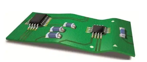
The main causes of PCB board bending and warpage are as follows:
PCB boards experience temperature changes during the reflow soldering process, generating thermal stress. Thermal stress can cause PCB board deformation.
The material properties of the PCB board also affect its likelihood of deformation. For example, materials with a large coefficient of thermal expansion are more prone to deformation.
The design of the PCB board also affects its likelihood of deformation. For example, the larger and heavier the board, the more likely it is to deform.
To prevent PCB board bending and warpage, the following measures can be taken:
Temperature control: Precisely controlling the temperature of the reflow oven is key to preventing deformation caused by thermal stress.
Use a reflow oven with a smaller temperature gradient to avoid abrupt temperature changes and reduce the impact of thermal stress on the PCB board.
Preheating stage: During the preheating stage of the reflow oven, gradually increase the temperature to ensure that the entire PCB board is heated evenly. This helps slow down the generation of thermal stress.
Cooling stage control: Control the speed of the cooling stage to avoid rapid cooling causing thermal shrinkage, which can lead to board warpage. Gradual cooling helps reduce thermal stress.
Thermal design: At the PCB design stage, consider adopting thermal design, that is, by adjusting the shape and material distribution of the PCB board to make it more stable during the SMT reflow process.
Material selection: Choose materials with a small coefficient of thermal expansion to reduce the impact of thermal stress. Materials with good rigidity can also reduce the possibility of PCB board bending and warpage.
Process optimization: During manufacturing, adopt low-temperature lamination processes, uniform heating reflow soldering processes, and low-force drilling processes to reduce the impact of mechanical stress and thermal stress.
Deformation inspection: After PCB board production is completed, perform deformation inspection to promptly discover and address any problems that may cause bending and warpage.
Through the above comprehensive improvement measures, bending and warpage of PCB boards during the reflow oven process can be more effectively prevented, ensuring the production of high-quality, highly stable electronic products.