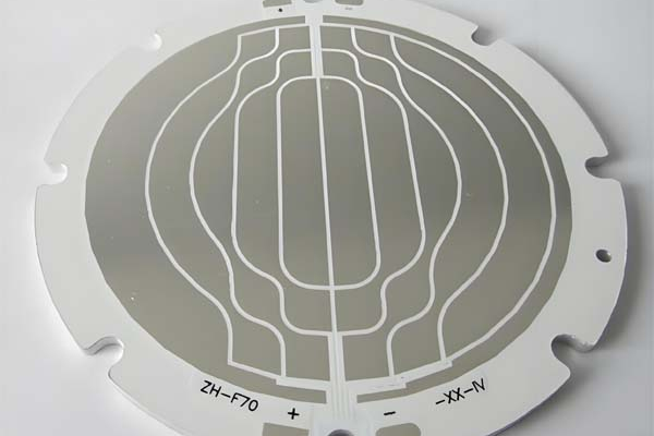
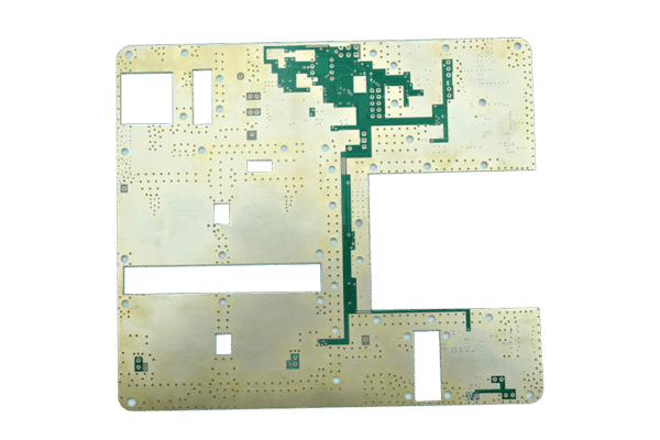
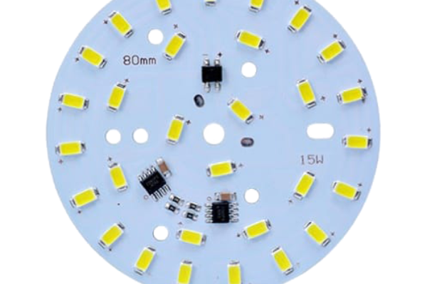
Before designing a PCB, we must understand the PCB layout process. Below is a detailed explanation:
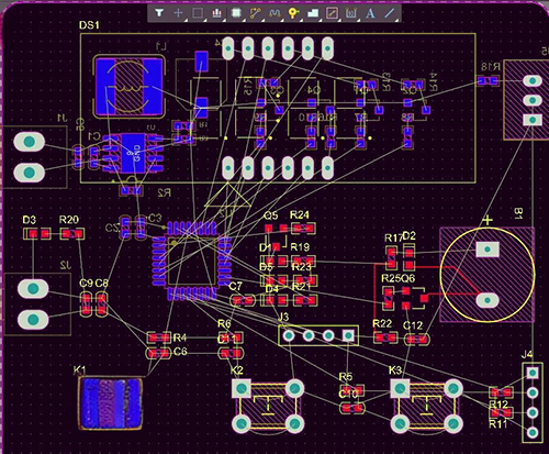
1. Draw the correct schematic and netlist.
The schematic is the prerequisite for PCB design, and the netlist is the bridge connecting the schematic and the PCB layout.
2. Determine component footprints and complete the conversion from schematic to PCB.
Altium designer provides a rich standard component library. Before importing the netlist file, the PCB footprint libraries must be loaded first to ensure that all required libraries have been loaded.
3. Set environmental parameters.
Set environmental parameters according to your own habits, such as grid size, cursor snap size, conversion between metric and imperial units, etc. In addition, the layers of the PCB board must also be set.
4. Plan the circuit board.
This mainly involves setting various physical parameters of the board, including whether the board uses a double-sided or multilayer board, the shape and dimensions of the board, the mounting method, etc.
5. Import the netlist.
The netlist contains the footprint/package type of each component and the connection relationships between components. Importing the netlist provides the basis for subsequent PCB design.
6. Component placement.
First place components related to mechanical dimensions and lock them, then place larger components that occupy more space and the core components of the circuit, and finally place the peripheral small components.
7. Formulate detailed routing rules.
Routing rules include trace spacing, various trace widths, via sizes, routing topology, etc., and need to be set according to the actual design. In addition, a fill layer should be placed in areas where routing is not desired.
8. PCB routing.
This step includes three stages: manual routing, autorouting, and manual adjustment.
9. Processing the lead-out terminals of the circuit board.
In the design, terminals such as power, ground, and signal input and output must be connected to the outside world. The lead-out method depends on process requirements. Common lead-out methods are lead-out using pads and lead-out using connectors.
10. Copper pouring and teardrop addition.
To enhance the board’s anti-interference capability, copper pouring must be performed on the ground network placed on each routing layer. In addition, teardrops need to be added to all vias and pads.
11. Perform a design rule check.
To ensure that the PCB layout complies with the design rules and that all nets are correctly connected, a design rule check must be performed after routing is completed.
12. Adjust the information on the remaining layers.
After passing the design rule check, drag all silkscreen characters to appropriate positions, and finally add information such as the board name, design version number, company name, and the date the file was first processed.
13. Save and export the PCB file.
After the design is completed, the PCB file should be organized, archived, and printed. In addition, a component list can be exported and a spreadsheet document can be generated as a component inventory, etc.