Obviously, in a microcontroller project, almost everything is based on the circuit board. The microcontroller and various components are soldered onto the circuit board, and the program is also written into the microcontroller on the circuit board. Therefore, the design and fabrication of the circuit board are the foundation of microcontroller projects.
The first step in doing anything is to be clear about the process. The figure above shows the general process of circuit board design. In fact, circuit board design is not difficult. Usually, first draw the component libraries for the components to be used (the component libraries include the schematic library and the footprint library), then draw the schematic, then generate an initial PCB layout based on the schematic, and then complete the final PCB layout through placement and routing. The entire design process is like this.
Table of Contents
Drawing Component Libraries:
Circuit board design generally includes these elements: components, layout, and routing. Among them, components are the foundation, just like the bricks used when building a high-rise building. Without bricks, a building cannot be built; without components, a circuit board cannot be made.
Altium designer comes with some component libraries, but they may not fully cover design requirements, so in many cases you need to design component libraries yourself.
Component library design includes two aspects: drawing the schematic library and the footprint library. To do these well involves several tasks: drawing component schematic symbols, designing component footprints, and binding them.
The schematic library is a collection of schematic symbols for various components. A component’s schematic symbol includes information such as the component name, appearance, and pins.
The footprint library is a collection of information including how each component is mounted and soldered on the PCB. Simply put, a component footprint is the part of the component that matches the soldering position on the circuit board, including elements such as the component outline, pads, or pins.
Binding means that after the component’s schematic symbol and footprint are drawn, the two need to be bound together so that they can call each other, making it convenient to draw subsequent schematics and PCB diagrams later.
Drawing the Circuit Schematic:
The circuit schematic is a principle-level drawing used to better understand and read the entire circuit. Drawing the circuit schematic means organizing the hardware required on the circuit board (generally represented by component schematic symbols) according to rules and drawing it on the diagram. A schematic is not a real circuit board diagram. For many experts, it may be possible to skip the schematic and directly draw the PCB diagram, but for most developers, the schematic is very meaningful for design and checking.
Drawing the PCB Diagram
Drawing the schematic mainly includes several aspects of work: component placement, component layout, and wiring.
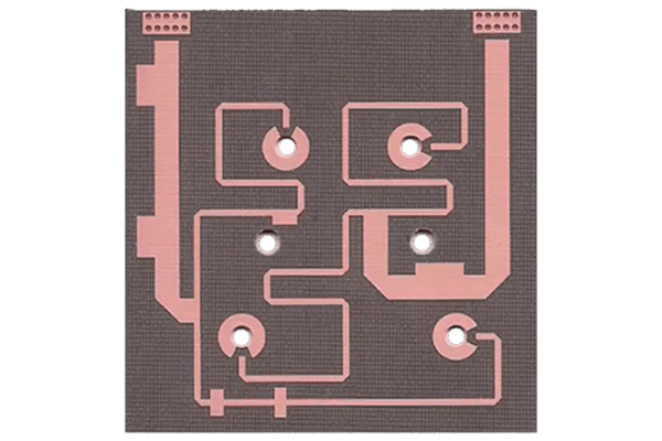
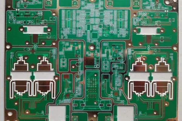
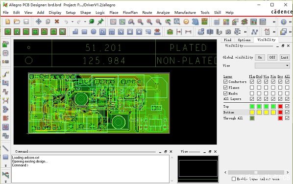
The final circuit board design still requires drawing the PCB diagram. The PCB diagram is basically exactly the same as the circuit board: whatever it is drawn like is what the manufactured circuit board will look like. It includes information such as component mounting positions, soldering pins, and routing between components.
Drawing the PCB diagram includes several tasks: placing components, component layout, and wiring. Here, components refer to component footprints. During component layout, many factors need to be considered, such as shortest routing, high-frequency and low-frequency isolation, analog and digital isolation, etc. During wiring, factors such as different trace widths and spacing for different devices and optimal routing also need to be considered.
The design of a typical circuit board basically consists of these contents. However, these tasks are based on relatively rich knowledge of electrical, analog circuit, and digital circuit principles, which requires time and accumulation to do well.
Conclusion:
Mastering the standard PCB design process and building strong circuit fundamentals are essential for producing reliable microcontroller projects. Although the workflow is straightforward, high-quality PCB design depends on careful component library preparation, clear schematics, thoughtful layout, and disciplined routing—skills that improve through experience and continuous practice.