To ensure high-performance design of PCBs, multi-dimensional system control is required, including material selection, layout and wiring, signal integrity, thermal management, manufacturing processes, and more. The following are key strategies based on cutting-edge technologies and practices in the industry:
Table of Contents
1、 Accurate material selection lays the foundation for performance
1. Optimization of substrate materials
-High frequency scenarios (such as 5G base stations and millimeter wave radars) prioritize the use of materials with low dielectric constant (Dk) and low loss factor (Df), such as Rogers RO4835 (Dk=3.48 ±) 0.05@10GHz )Or MEGTRON7 (Df= 0.0015@10GHz )It can significantly reduce signal attenuation.
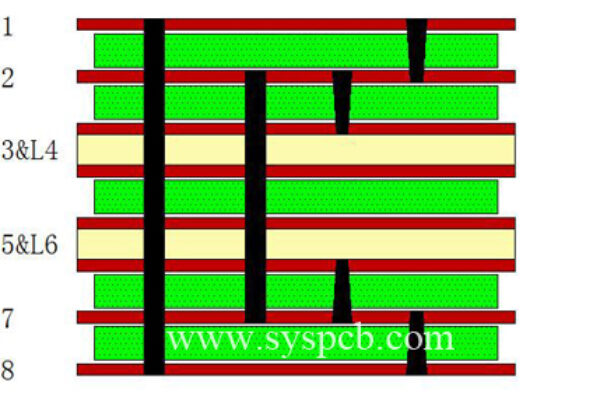
-High multilayer boards (8 or more layers) are made of Taiwan South Asia or Shengyi high-frequency materials (Tg ≥ 170 ℃, Dk=3.8), Ensure stability in high temperature environments.

-Under the trend of environmental protection, halogen-free FR-4 (CTI ≥ 600V) and bio based epoxy resin (reducing carbon footprint by 65%) have become mainstream choices.
2. Copper foil and surface treatment
-The high-speed signal path adopts Reverse Processing (RTF) copper foil (roughness<0.5 μ m), which can reduce the insertion loss in the 28GHz frequency band by 0.15dB/inch.
-Surface treatment selection based on application: ENIG (gold layer 0.025-0.127 μ m) is suitable for BGA packaging, while HASL (lead-free Sn Ag Cu alloy) has lower cost but higher roughness.
2、 Layout and wiring strategy to enhance signal integrity
1. Partition layout and key component positioning
-Partition and isolate high-frequency, analog, and digital circuits, and keep key components (such as processors and memory) as close as possible to shorten the signal path.
-Clock signals and differential pairs (such as USB4 and PCIe 6.0) need to be processed in a grounded manner and kept away from high current paths to reduce EMI.
2. Guidelines for high-speed signal wiring
-Differential pairs are strictly equal in length (with an error of less than 5ml), impedance matched (such as USB4 with 90 Ω), and avoid cross segmentation and layer swapping vias to ensure a continuous reference plane.
-PCIe 6.0 uses PAM4 modulation and 1280/1302 encoding, requiring control over the routing length (single end ≤ 1800mil) and the number of via holes, in conjunction with optimizing signal return through via holes.
3. Power and ground plane design
-The power layer is adjacent to the ground layer to reduce parasitic inductance, and decoupling capacitors (0.1 μ F ceramic capacitors) are evenly distributed according to the principle of “placing one capacitor every 10mm ²”, close to the chip power pin.
-When using a segmented ground plane, the digital ground and analog ground are connected at a single point through a 0 Ω resistor to avoid noise coupling.
3、 Thermal management technology ensures long-term reliability
1. Design of heat dissipation structure
-Lay large-area heat dissipation copper foil under high-power components such as IGBT and FPGA, and conduct heat to the inner layer or heat sink through dense thermal vias (aperture ≥ 0.3mm).
-The thermal conductivity of ceramic filled substrate (AlN content 40%) reaches 4.5W/m · K, which can reduce the junction temperature by 28 ℃; Graphene composite materials achieve directional heat dissipation and are suitable for high heat scenarios such as blade servers.
2. Thermal simulation and material matching
-Perform thermal analysis using ANSYS or Mentor Graphics to optimize temperature distribution. In SiP packaging, the gradient copper pillar structure (CTE gradient difference<0.5ppm/℃) can buffer the thermal expansion mismatch between the chip and the substrate, extending the solder joint life to 10 ^ 8 cycles.
4、 Manufacturing Process and Design for Manufacturability (DFM)
1. High precision machining capability
-The mainstream process achieves a line width and spacing of 3-4mil, and LDI laser direct imaging technology supports fine wiring of 3mil on 2nd order HDI boards with impedance tolerance of ± 10%.
-The minimum aperture of the through-hole is 0.15mm, and the laser drilling blind hole reaches 0.1mm. The uniformity error of the copper plating layer is ≤± 5 μ m.

2. Local manufacturing resources in Dongguan
-SysPCB’s military grade production line supports 24-hour fully automated production, with a yield rate of 98.5% for soft and hard combination boards and a bending life of over 100000 times.
-The annual water saving of the closed-loop water system is equivalent to 30 standard swimming pools, which meets the EU’s WEEE 2025 environmental protection requirements.
5、 Simulation verification and testing process
1. Design phase simulation
-Use SIwave for power integrity analysis, HFSS for electromagnetic compatibility verification, and ANSYS RedHawk for thermal simulation to detect impedance mismatch, crosstalk, and other issues in advance.
-AI tools, such as Yibo Technology’s intelligent design platform, can optimize layout and shorten research and development cycles by more than 30%.
2. Mass production testing and compliance
-FPT detects open/short circuits, 3D AOI identifies 0.02mm defects, and ICT online testing coverage is greater than 95%.
-Automotive electronic boards need to pass IATF16949 certification and work stably for 3000 hours in an environment of 85 ℃/85% RH.
6、 Frontier Technologies and Industry Trends
1. High speed interface design

-PCIe 6.0 supports 64 GT/s transmission and requires low jitter clock and equalization circuit. The connector should be selected as M.2 or U.2 to meet high-density requirements.
-The differential line of USB4 should prioritize the inner layer, and the return path should be complete to avoid impedance jumps caused by cross segmentation.
2. Green Manufacturing and Sustainability
-Following the new regulations of WEEE 2025, modular design (DfR) and easy to disassemble soldering materials are adopted, with a PCB recycling rate of 85% and a material reuse rate of ≥ 50%.
-Biobased epoxy resin and lead-free solder (such as Sn Ag Cu) have become mainstream, reducing carbon footprint and complying with RoHS 2025 standards.
7、 Reference for practical application cases
-5G base station RF board: Using Rogers 4350B substrate and 1.8 μ m gold deposition process, the insertion loss in the 10GHz frequency band is less than 0.15dB/cm, and has passed temperature cycling tests from -55 ℃ to+125 ℃.
-AI toy voice module: 6-layer board design, single point connection between analog and digital ground, I2S bus length error<5mil, meets EN 62115 electromagnetic safety certification.
Through the above strategies, SysPCB, combined with Dongguan’s mature supply chain and advanced manufacturing capabilities, can systematically improve the electrical performance, reliability, and environmental adaptability of PCBs, meeting the stringent requirements of high-end electronic devices.
Get your exclusive quote immediately: fill out the form or send an email directly.As a professional PCB manufacturer for hobbyist , we will provide you with a quote service within 24 hours. Enjoy free DFM optimization and a 10% discount on SMT patches for your first order!