Designing and assembling your own Printed Circuit Board (PCB) can be a rewarding experience, allowing for greater customization and a deeper understanding of electronics. This guide covers the essential steps involved in DIY PCB design, fabrication, and soldering to help you create functional and reliable circuit boards.
Table of Contents
1. PCB Design
The first step in making a DIY PCB is designing the circuit layout. This involves:
Choosing Design Software: Popular PCB design tools include KiCad, Eagle, and Altium Designer.
Creating the Schematic: Define the circuit connections and components.
Laying Out the PCB: Arrange components and traces to optimize performance and minimize interference.
Generating Gerber Files: These files are required for PCB fabrication and should be exported according to manufacturer specifications.
2. PCB Fabrication
Once the design is complete, the PCB needs to be fabricated. There are two common methods:
a. Professional Fabrication
Submit your Gerber files to a PCB manufacturer.
Choose specifications such as board thickness, copper weight, and surface finish.
Wait for delivery and inspect the PCB upon arrival.
b. DIY Etching Method
For small-scale projects, PCBs can be etched at home:
Print the PCB Layout: Use a laser printer to print the design onto glossy paper.
Transfer the Design: Use a clothes iron to transfer the toner onto a copper-clad board.
Etching Process: Immerse the board in a ferric chloride solution to remove unwanted copper.
Drilling and Finishing: Drill holes for through-hole components and clean the board.
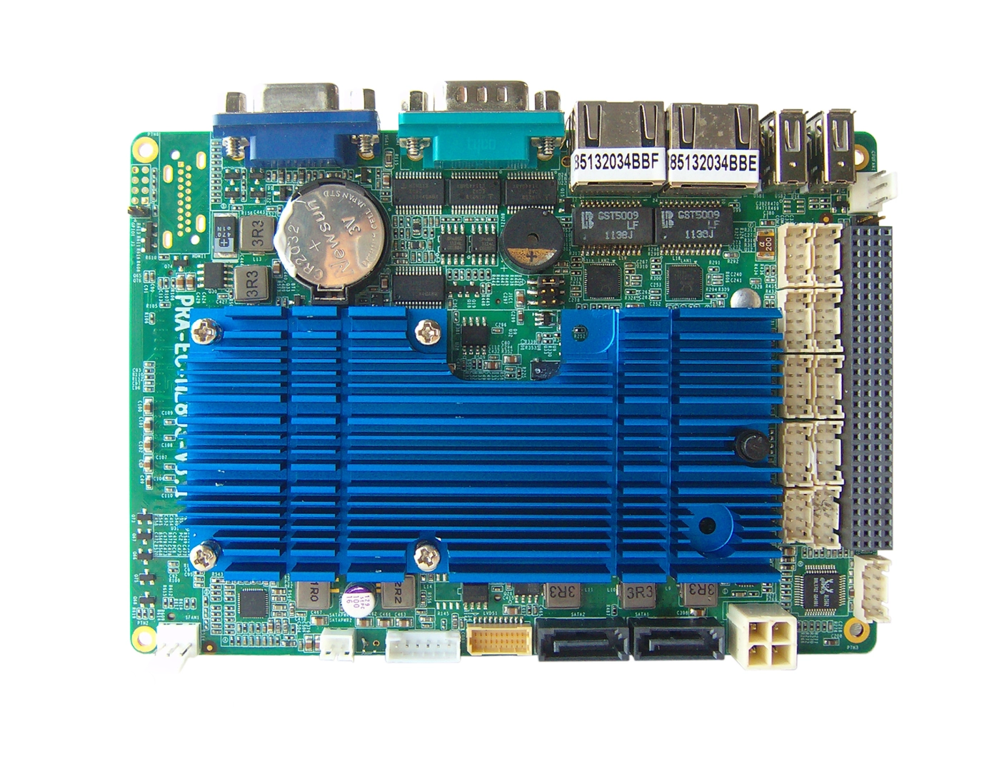
3. Soldering Components
Once the PCB is ready, components need to be soldered onto it.
a. Required Tools
Soldering iron (temperature-controlled for better precision)
Solder wire (preferably lead-free for safety)
Flux (improves solder flow and prevents oxidation)
Tweezers and desoldering tools for adjustments
b. Soldering Techniques
Through-Hole Soldering: Insert component leads through the board and solder them from the opposite side.
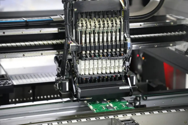
Surface Mount Soldering (SMT): Use fine-tip soldering irons or reflow techniques for tiny components.
Avoiding Cold Joints: Ensure the solder fully melts and bonds with the pad and component lead.
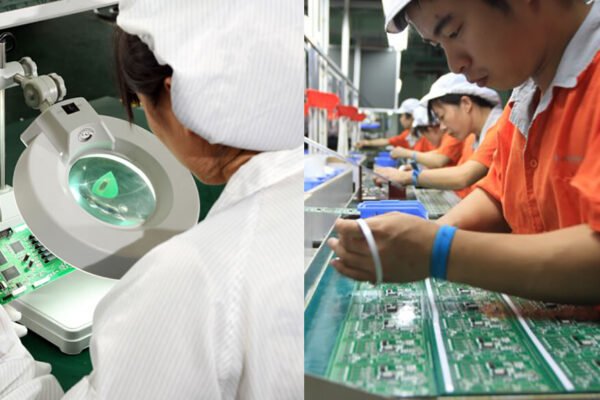
4. Testing and Troubleshooting
Before using the PCB, verify its functionality:
Visual Inspection: Check for solder bridges or misaligned components.
Multimeter Testing: Measure continuity and resistance to ensure proper connections.
Powering Up: Use a current-limited power supply to prevent damage in case of faults.
Debugging: If the circuit does not work, check for errors in soldering or component placement.
Conclusion
DIY PCB design and soldering can be an exciting and educational process. By following proper design principles, fabrication methods, and soldering techniques, you can create reliable PCBs for personal or professional projects. With practice, you can improve your skills and even experiment with advanced techniques such as reflow soldering and multilayer PCBs.