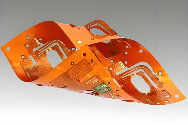
In PCB design, there are usually multifarious PCB special components, and the layout of these special components is also very particular.
When designing how to place special components, first consider the size of the PCB. When the PCB size is too large, the printed lines will be too long, the impedance will increase, the resistance to interference will decrease, and the cost will increase; if it is too small, the heat dissipation will not be good, and adjacent lines will be easily interfered. After determining the PCB size, determine the position of the special component. Finally, array all components of the circuit according to functional units.
The location of special components should generally follow the following principles when layout:
1. Try to shorten the connection between high-frequency components, minimize their distribution parameters and mutual electromagnetic interference. Components that are susceptible to interference should not be too close, and the input and output should be as far away as possible.
2. Some components or wires may have a high potential difference, so the distance between them should be increased to avoid accidental short circuits caused by discharge. High-voltage components should be placed out of reach as much as possible.
3. Parts weighing more than 15g can be fixed with brackets and then soldered. These heavy and hot components should not be placed on the circuit board, but on the shell bottom of the main box, and heat dissipation should be considered. Keep heat sensitive parts away from heating components.
4. For the layout of adjustable components such as potentiometers, adjustable inductance coils, variable capacitors and micro switches, the structural requirements of the entire board should be considered. If the structure allows, some commonly used switches should be placed in a position that is easily accessible by hand. The layout of the components should be balanced. The success of a product must firstly focus on the internal quality, and secondly, consider the overall aesthetics. And board that combines both can be a successful product.
PCB special components refer to the key components of the high-frequency part, the core components in the circuit, the susceptible components, the high-voltage components, the high-calorific value components, and some heterogeneous components. It is necessary to carefully analyze the location of these special components to make the layout meet the circuit function and production requirements. Improper placement may cause circuit compatibility issues and signal integrity issues, leading to PCB design failures.