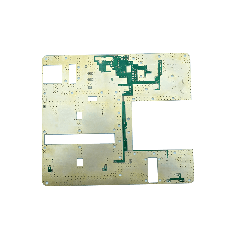
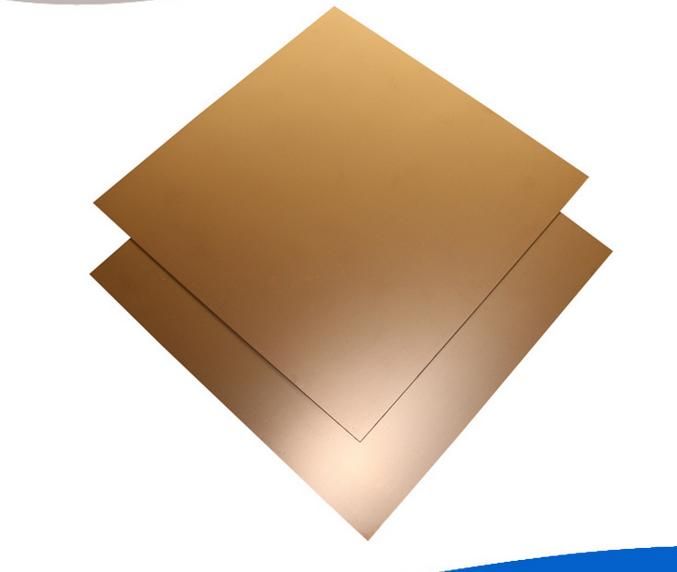
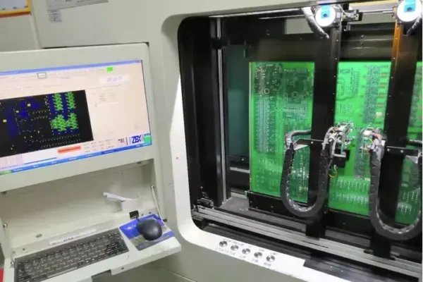
High frequency antennas (such as antennas for 5G, millimeter wave, satellite communication, radar, and other scenarios) have much higher performance requirements for PCB materials than ordinary low-frequency circuits. The core requirements are to reduce signal loss, ensure phase stability, improve antenna efficiency, and adapt to physical and environmental stresses in high-frequency environments. The following are the key characteristics and common types of high-frequency antenna PCB materials:
Table of Contents
Ⅰ. Core characteristics required for High frequency Antenna PCB material
High frequency antennas operate in the GHz range (even millimeter waves such as 24GHz, 60GHz, 77GHz, etc.), with extremely short signal wavelengths (centimeter to millimeter range). Even small changes in material properties can significantly affect key indicators such as resonant frequency, gain, and standing wave ratio (VSWR) of the antenna. Therefore, the material needs to meet the following core characteristics:

1. Excellent electrical performance (core indicator)
-Low and stable dielectric constant (Dk)
The dielectric constant (Dk) is the ability of a material to store electric field energy, which directly affects the size of the antenna (wavelength λ is inversely proportional to √ Dk, the larger the Dk, the smaller the antenna size can be at the same frequency, but stability needs to be balanced).
Key requirements: ① The Dk value should be stable and uniform (with high consistency within and between boards) to avoid antenna performance dispersion caused by uneven materials; ② The variation with frequency and temperature is small (Dk drift at high frequencies should be ≤ 0.02, temperature coefficient ≤ 50ppm/℃), otherwise it will cause the resonant frequency of the antenna to shift.
-Extremely low dielectric loss (Df)
Dielectric loss (Df) is an indicator of the energy consumption of materials due to molecular polarization at high frequencies, which directly determines signal attenuation (the smaller the tangent of the loss angle, the less energy loss).
High frequency antennas (especially in long-distance communication or high gain scenarios) need to have a Df as low as possible (usually requiring Df ≤ 0.005, and in millimeter wave scenarios it should be ≤ 0.002), otherwise it will lead to a decrease in antenna efficiency and gain.
2. Good mechanical and dimensional stability
-Low coefficient of thermal expansion (CTE)

High frequency antennas require extremely high physical dimensional accuracy (millimeter or even micrometer level), and the thermal expansion coefficient of the material needs to match that of copper foil (copper’s CTE is about 17ppm/℃). Otherwise, temperature changes can cause PCB deformation and copper foil peeling due to thermal stress, thereby changing the physical dimensions of the antenna and damaging its resonance characteristics.
Requirement: CTE in the Z direction (thickness direction) should be ≤ 30ppm/℃, and CTE in the X/Y direction should be ≤ 20ppm/℃.
-High rigidity and deformation resistance
The material needs to have sufficient mechanical strength to avoid deformation during processing (such as drilling, cutting) or use (such as vibration, impact), ensuring the stability of the antenna’s geometric structure (such as radiating elements, feeder shapes).
3. Adapt to the characteristics of the environment and process
-Low water absorption
The dielectric constant of water is about 80 (much higher than PCB materials), and the absorption of water by the material can lead to a significant increase in Dk, a decrease in uniformity, and even oxidative corrosion. Require water absorption rate ≤ 0.1% (boiled in water for 24 hours).
-Good thermal conductivity
High frequency antennas (especially in high-power scenarios) generate heat due to current concentration, and the material needs to have a certain thermal conductivity (≥ 0.3W/m · K) to avoid performance drift or failure caused by local overheating.
-Compatibility with manufacturing processes
It is necessary to adapt to the conventional PCB processing flow (such as photolithography, etching, and lamination), and have strong adhesion with copper foil (especially ultra-thin electrolytic copper or rolled copper commonly used in high frequency) (peel strength ≥ 1.5N/mm) to avoid signal transmission path breakage.
4. Other scenario based requirements
-Radiation resistance/weather resistance: Materials for aerospace, automotive and other scenarios require resistance to ultraviolet radiation and high and low temperature impacts (-55 ℃~125 ℃ cycling);
-Lightweight: Low material density (≤ 2.0g/cm ³) is required for scenarios such as drones and satellites;
-Cost controllable: Consumer electronics (such as 5G mobile phone antennas) need to balance performance and cost.
Ⅱ. Common materials and characteristics of high-frequency antenna PCB
High frequency antenna materials can be divided into fluoropolymer based, polyimide based, modified epoxy resin based, etc. according to the substrate type. Among them, fluoropolymer has the best genetic and electrical properties and is the mainstream choice for high-frequency scenarios.
1. Fluoropolymer based materials (preferred for high frequency and top-notch performance)
Using PTFE (polytetrafluoroethylene, commonly known as “Teflon”) as the substrate and adding fillers such as glass fiber and ceramic powder to adjust Dk, it has excellent electrical performance and is the core material for millimeter wave and high-precision antennas.
-Features: Dk range of 1.9~10 (adjustable by filler), extremely low Df (0.0005~0.002), water absorption<0.01%, good temperature resistance (long-term use temperature -200~260 ℃), but high cost and difficult processing (requiring special lamination process).

-Typical model:
-Rogers: RO4003C (Dk=3.38, Df=0.0027, moderate cost, suitable for 5G base stations), RO5880 (Dk=2.2, Df=0.0009, preferred for millimeter wave), RT/duroid 5880 (no glass fiber, more uniform Dk, suitable for ultra precision antennas);
-Taconic: TLY-5 (Dk=2.2, Df=0.0009), TLX-8 (Dk=2.55, lower cost than Rogers);
-Panasonic: Megtron 7 (Dk=3.4, Df=0.0025, balancing performance and processability).
2. Polyimide based material (outstanding temperature resistance)
Using polyimide (PI) as the substrate, adding glass fiber or ceramic, balancing high-frequency performance and high temperature resistance, suitable for high-temperature environments (such as car radar near the engine).
-Features: Dk=3.0~4.5, Df=0.002~0.008 (slightly higher than PTFE), excellent temperature resistance (long-term use temperature ≥ 200 ℃), high mechanical strength, but slightly higher water absorption than PTFE (about 0.1~0.3%).
-Typical model:
-Rogers: Ultrasim (Dk=3.0, Df=0.003, suitable for high temperature and high frequency scenarios);
-DuPont: Kapton series (substrate, requiring composite copper foil).
3. Modified epoxy resin based materials (cost sensitive scenarios)
Improved resin based on traditional FR-4 (such as adding cyanate ester, polyphenylene ether, etc.) to reduce Df and enhance Dk stability, suitable for high frequency (1-10GHz) and cost sensitive scenarios (such as consumer electronics antennas).
-Features: Dk=3.8~4.5, Df=0.004~0.01 (higher than PTFE, but much lower than ordinary FR-4’s 0.02~0.03), cost is only 1/3~1/5 of PTFE based, and processing technology is compatible with conventional FR-4.
-Typical model:
-Shengyi: S1000-2 (Dk=3.8, Df=0.004, commonly used for 5G mobile phone antennas);
-TAIYO: TG170 (Dk=4.2, Df=0.006, suitable for small to medium power high-frequency antennas).
4. Ceramic based composite materials (ultra-high precision scenarios)
Using ceramics such as alumina and aluminum nitride as substrates, composite metal layers (such as copper and silver), with extremely high Dk (6-20) and excellent stability, suitable for ultra small antennas (such as millimeter wave chip antennas).
-Features: Dk stability (temperature coefficient ≤ 10ppm/℃), Df=0.001~0.005, But it has high brittleness, high processing difficulty, and extremely high cost, limited to special scenarios (such as aerospace radar).
Summarize
The core of high-frequency antenna PCB materials is “low loss, high stability, and adaptability to different scenarios”:
-PTFE based materials (such as Rogers RO5880) are preferred for millimeter wave and high-precision scenarios (such as satellites and radars);
-High temperature environments (such as near car engines) can choose polyimide based materials;
-Prioritize the modification of epoxy resin based materials (such as S1000-2) in consumer electronics and mid to high frequency (5G Sub-6GHz) scenarios, balancing performance and cost.
The selection of materials should be comprehensively judged based on antenna frequency, power, environmental requirements, and cost budget, and their performance directly determines the efficiency and reliability of the antenna.
Get your exclusive quote immediately: fill out the form or send an email directly.As a professional PCB manufacturer for hobbyist , we will provide you with a quote service within 24 hours. Enjoy free DFM optimization and a 10% discount on SMT patches for your first order!


